
Hello all! After a long distraction and period of satisfaction with my system, the itch has struck me again.
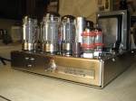
It was 7 years ago that I built my VTA SP12 with a PH12 included. It was one of the very first SP12 kits that Roy sold (possibly even the first SP12 not built by Roy, but I'm not entirely sure.) I had just added to VTA board to my Dynaco ST70, and knew I needed to get into Roy's other designs. Both Roy and Bob were great help as I dove into this hobby all those years ago, and they never fail to be a great resource when their help is needed. I would also be a fool to not mention how awesome it was to work with Kevin from Dynakit Parts too...couldn't have built my MKIIIs without him.
I've since built my own set of speakers, a design by Paul Carmody called 'Sunflowers.' They sound great! I then built a nixie tube chessboard lit by induction coils designed by Tony 'Lasermad' Adams from the UK, and I've completely rebuilt a set of Dynaco MKIII Monoblocks, adding Roy's driver board to them with octal 6SN7s. I also followed my tube obsession into amateur radio and became a ham a couple of years ago...so 73 from W8EFG.
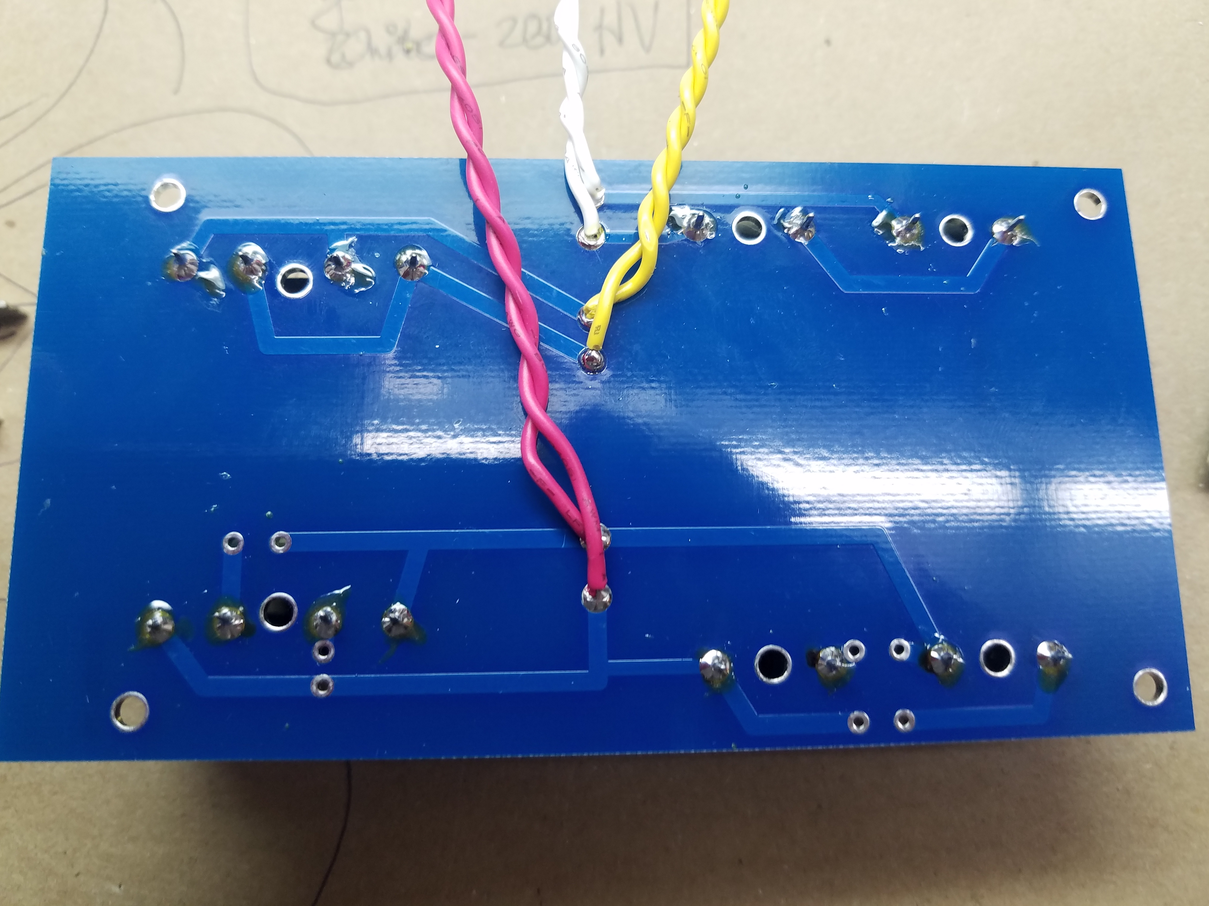
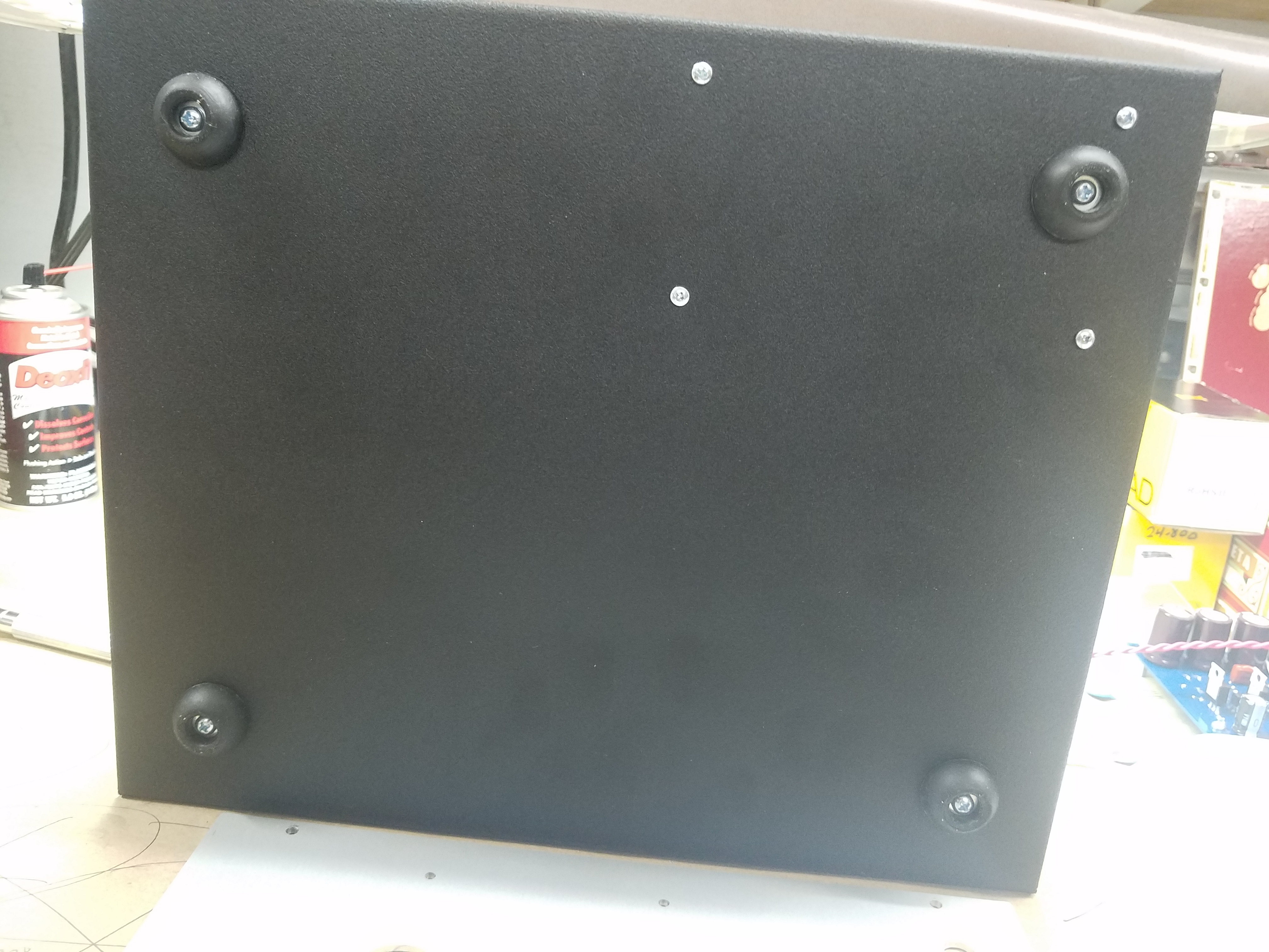
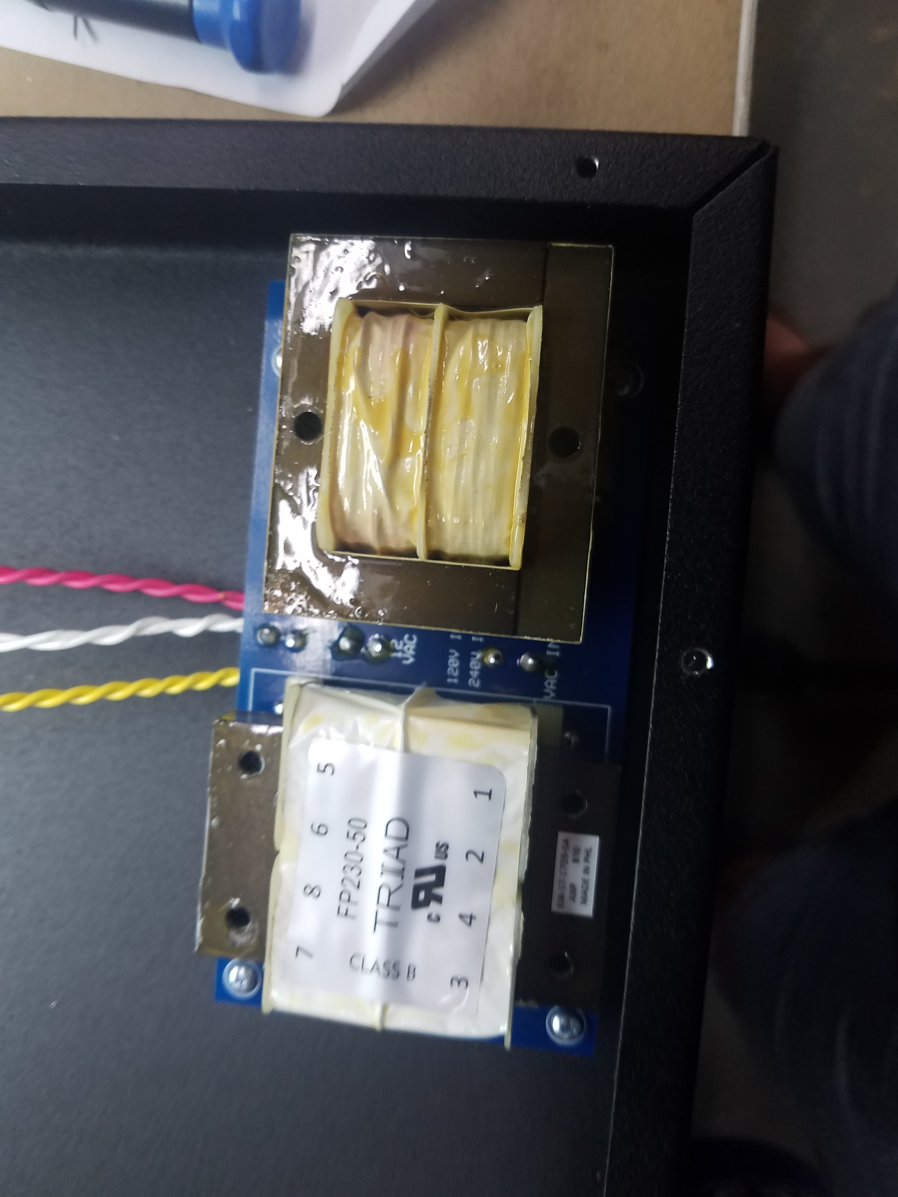
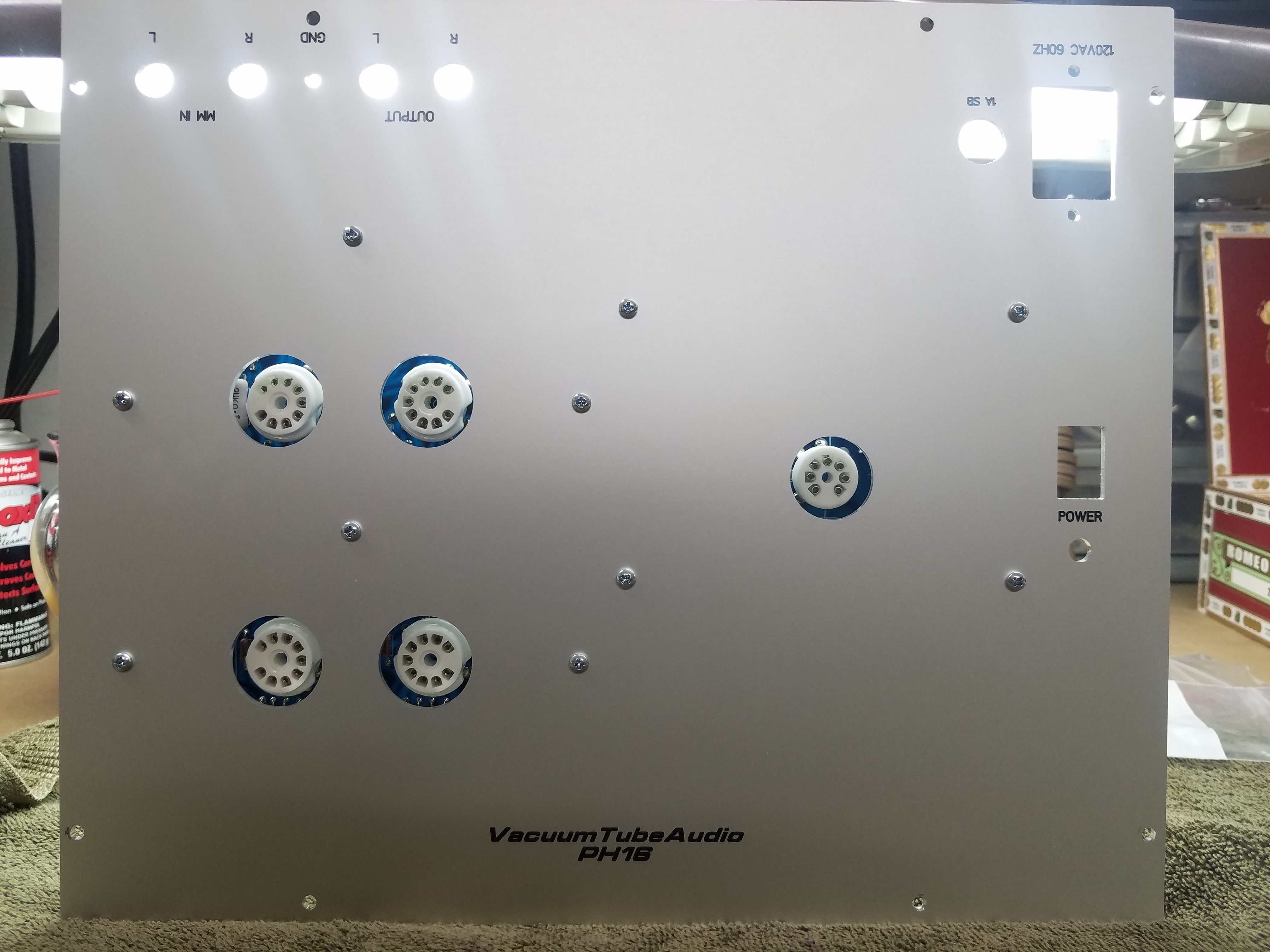
So........My birthday happened last weekend and my wife contacted Roy and bought me the PCB kit for the PH16X. AND she gave me permission to buy the rest of it as well as to squeeze in an SP14 kit too. Best birthday ever!!!
If the interest is here, I'll try to document as well as I can my build progress in this thread. Hopefully it can serve as a guide for someone who is doing their own build and give others an opportunity to learn from my mistakes and to tap the community for any help that I might need. If that goes well, I'll chronicle my SP14 build in the same fashion.
I am hosting my pics on my own server, and may take a few tries to get them to show properly. Be patient with me over the next 24 hours as I get that worked out.
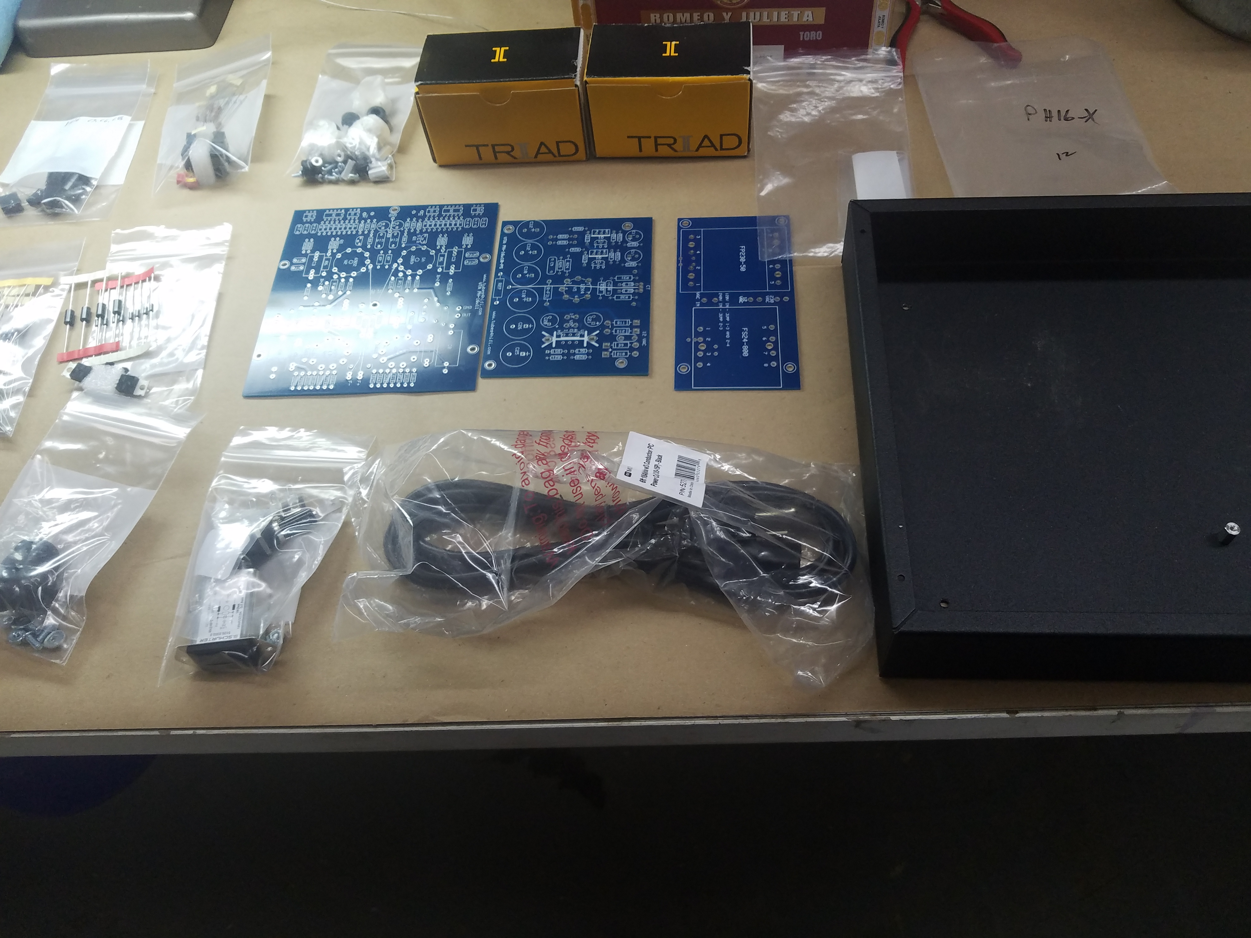
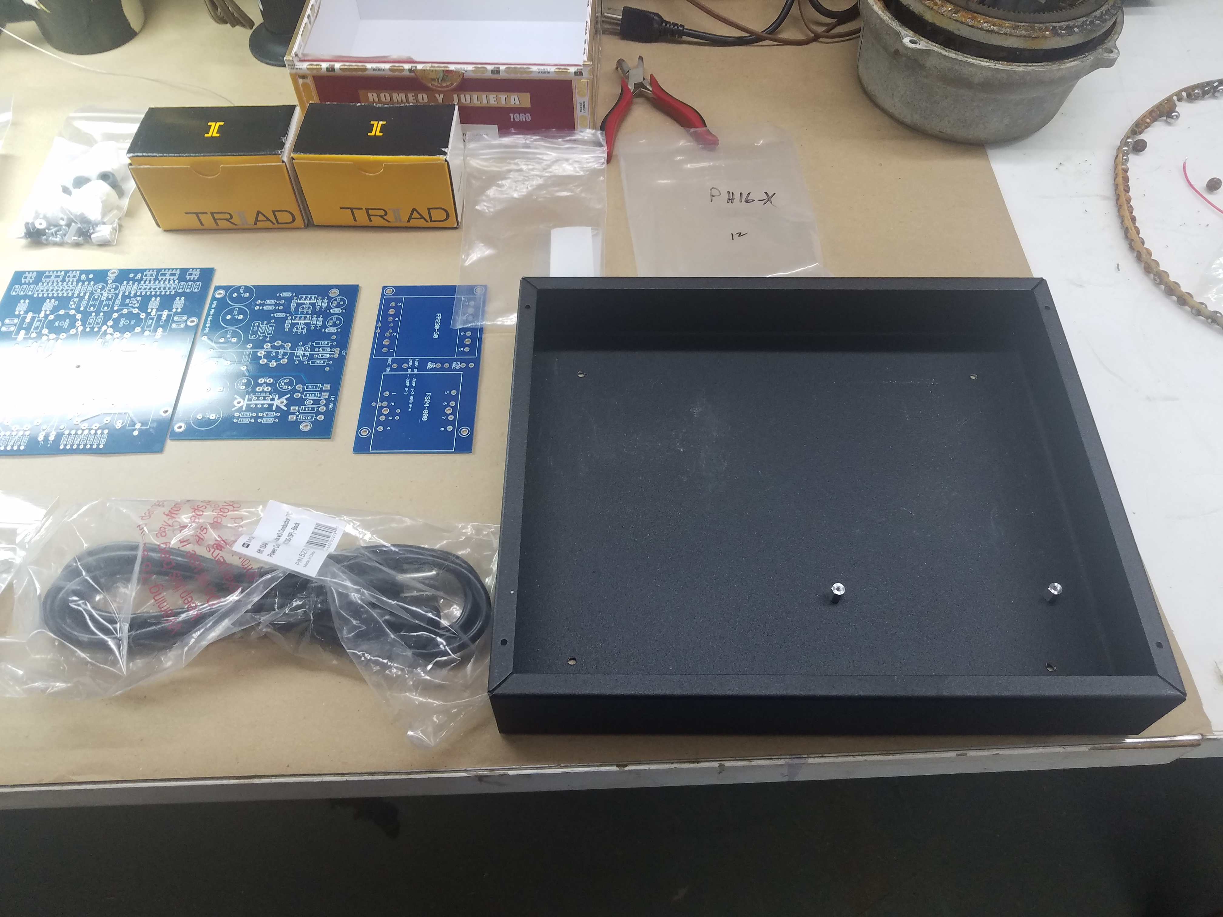
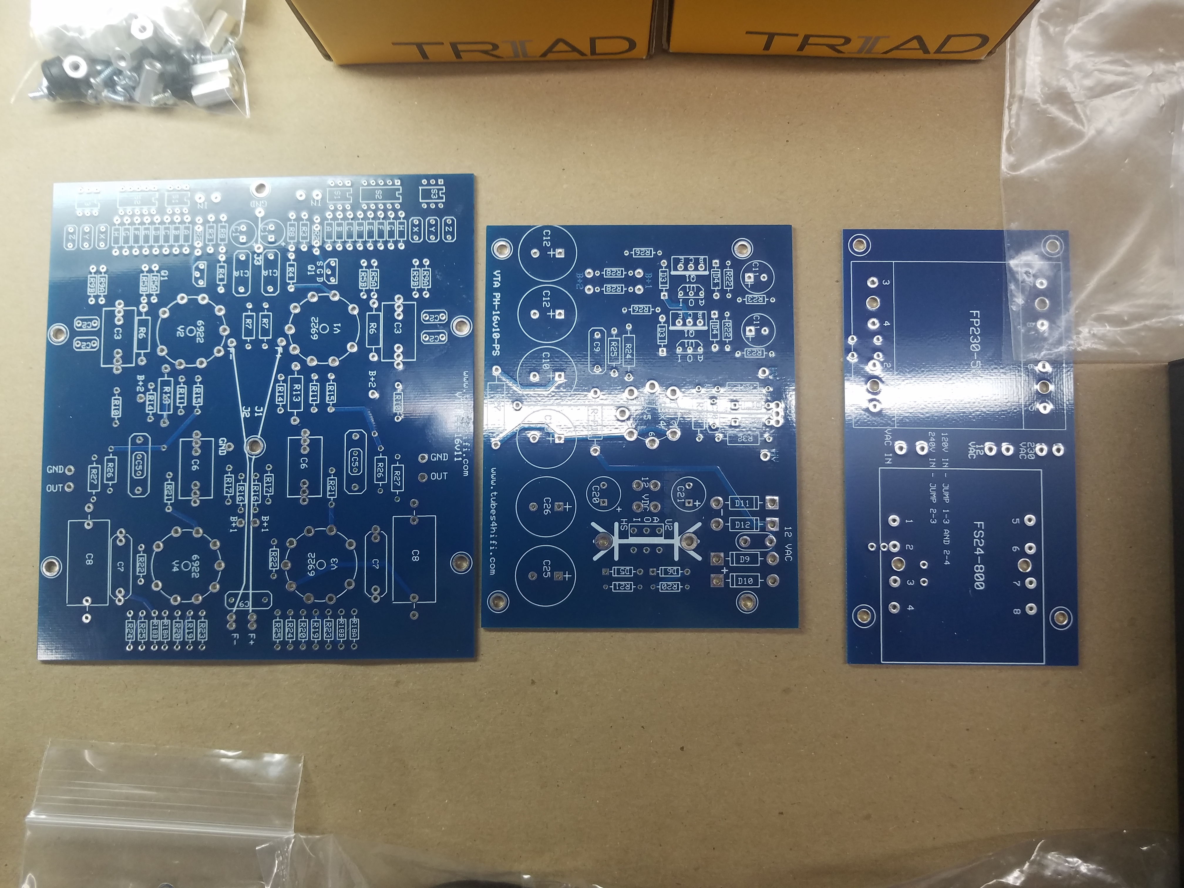
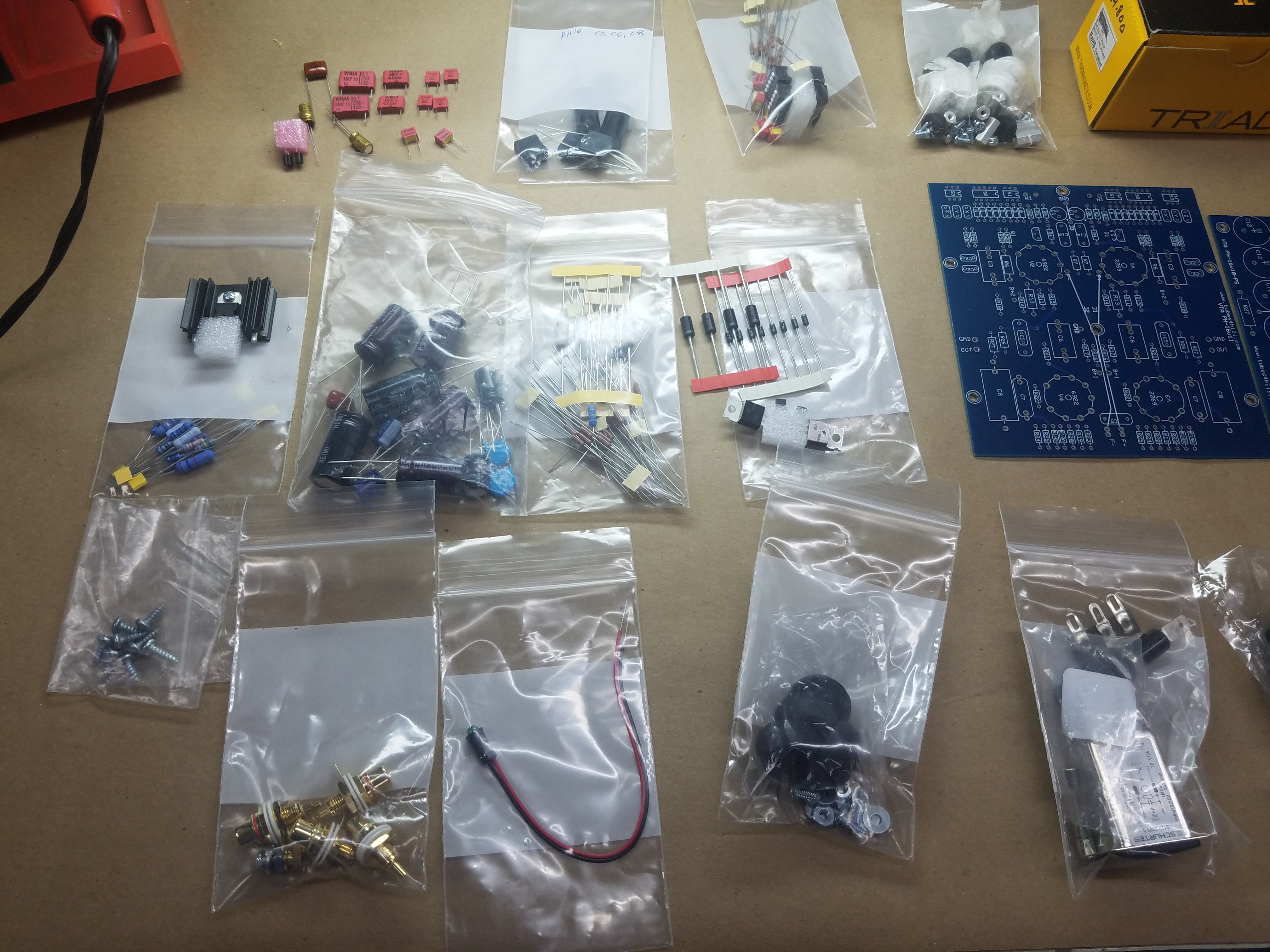
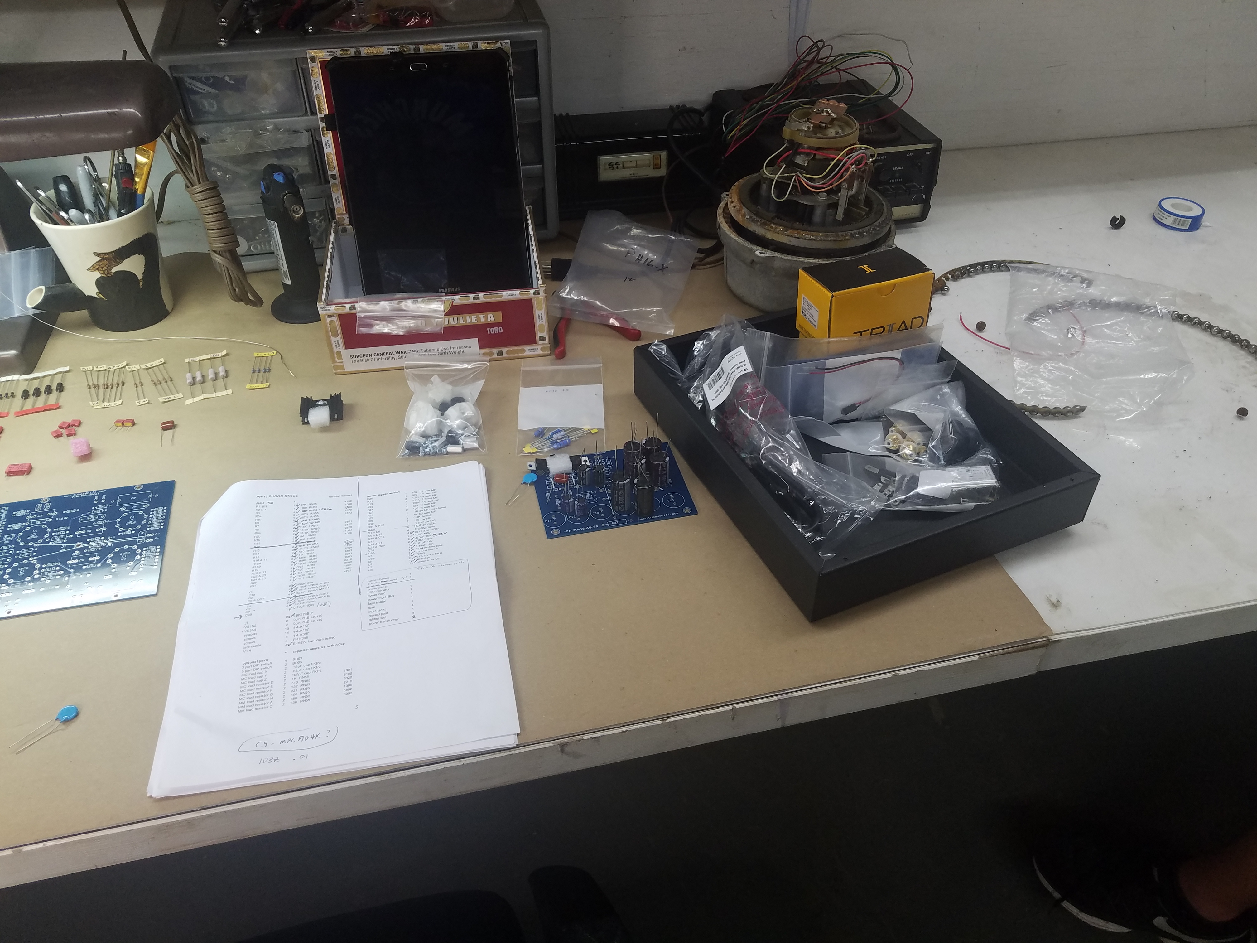
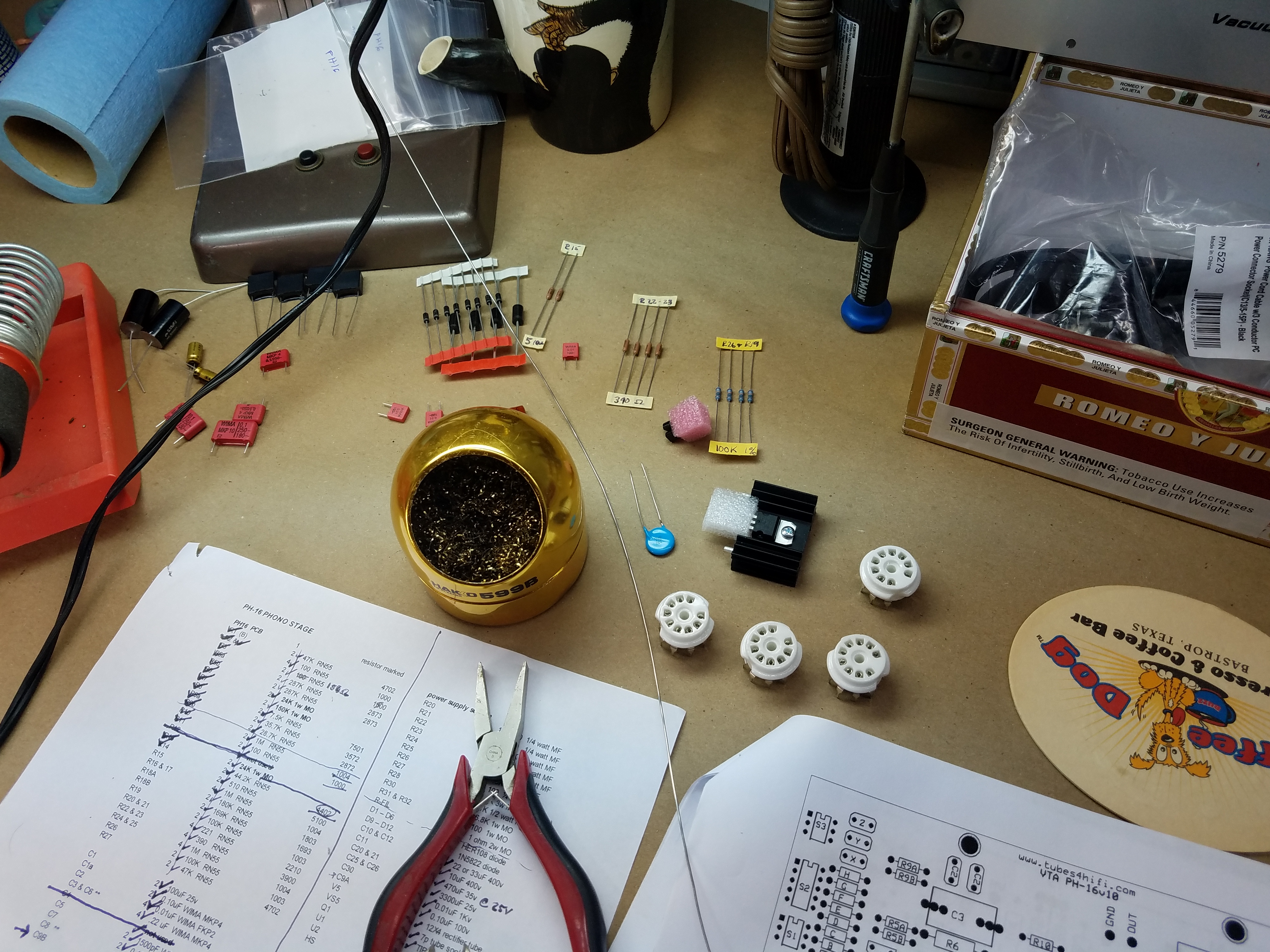
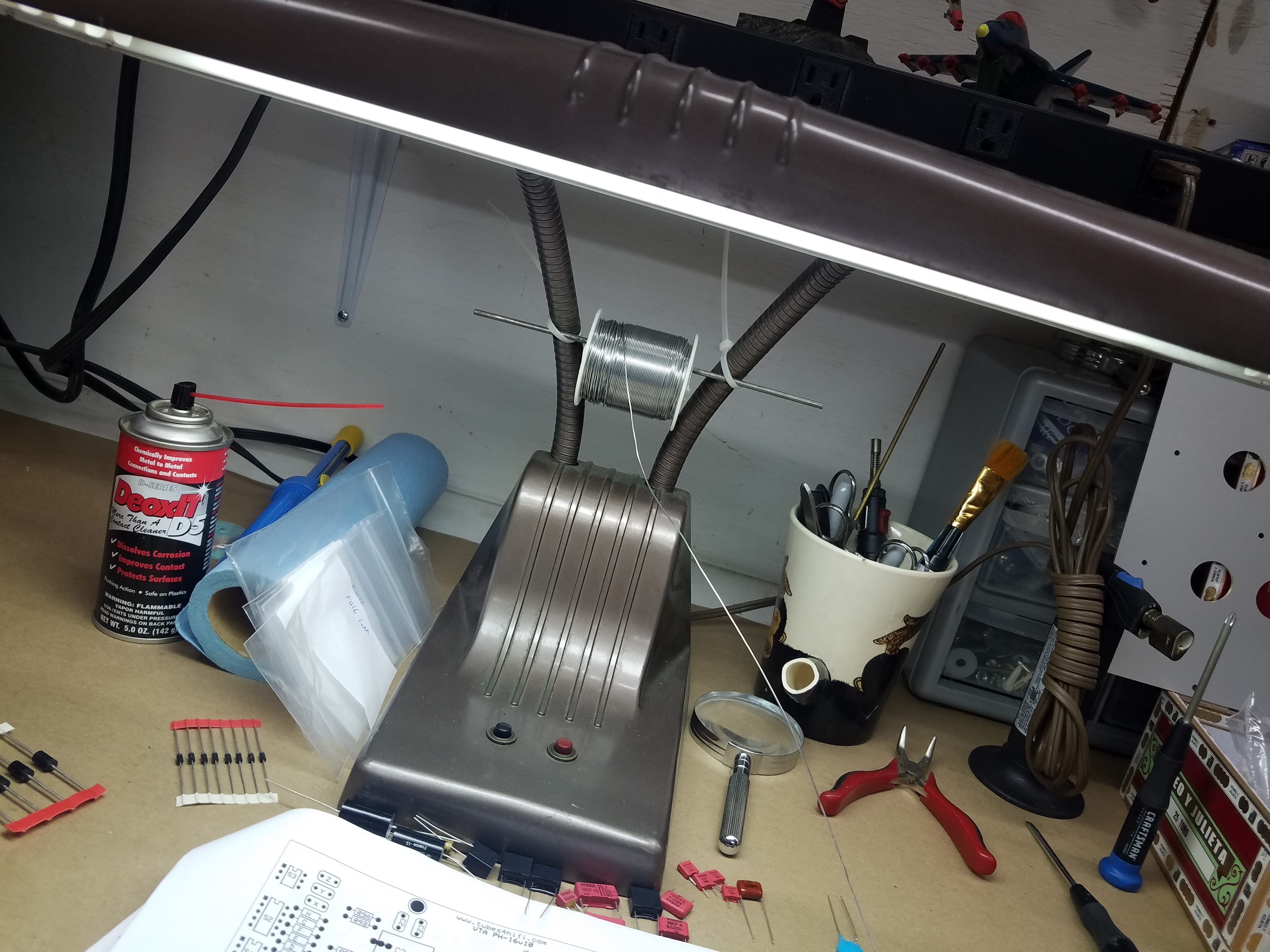
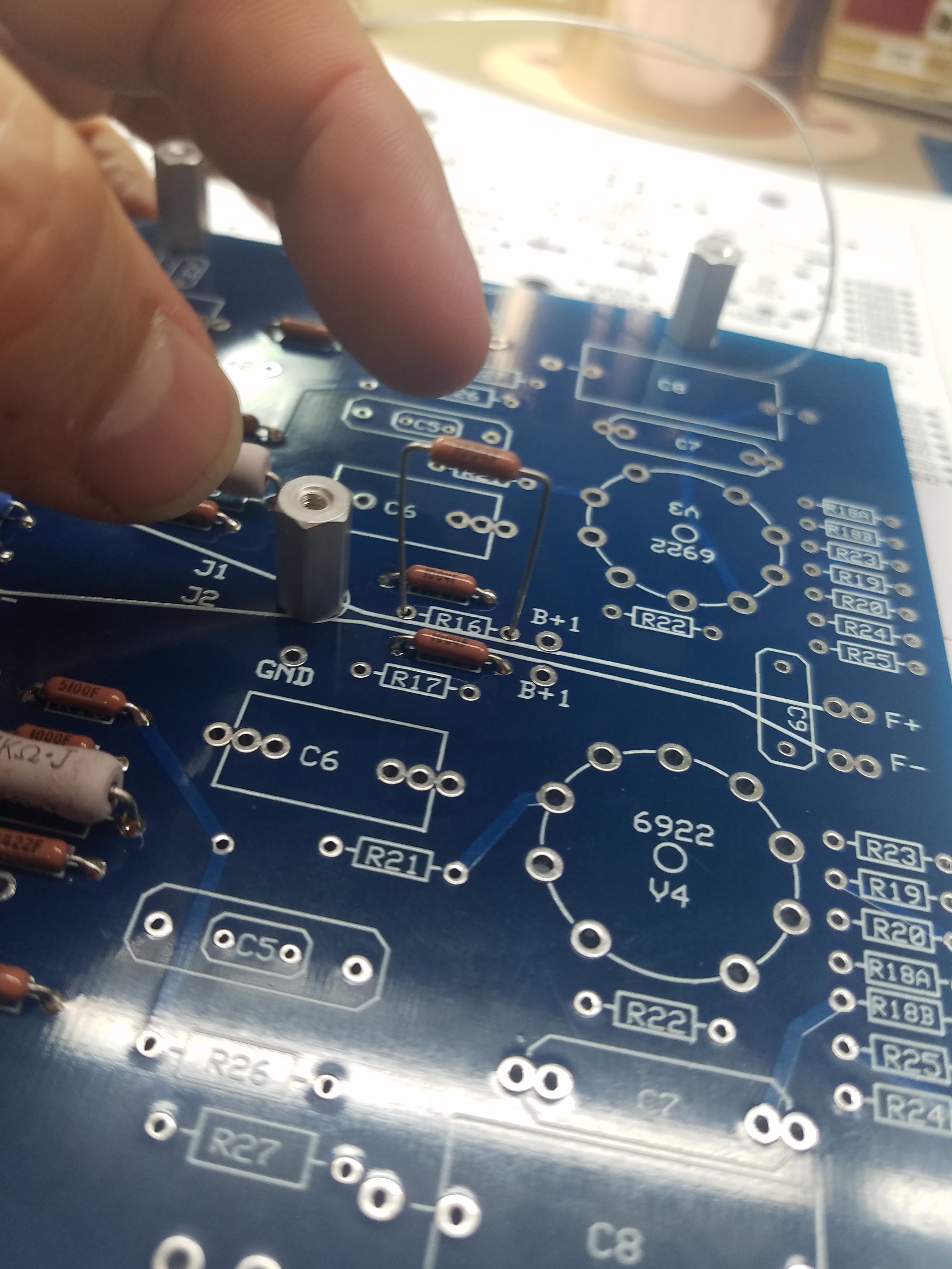
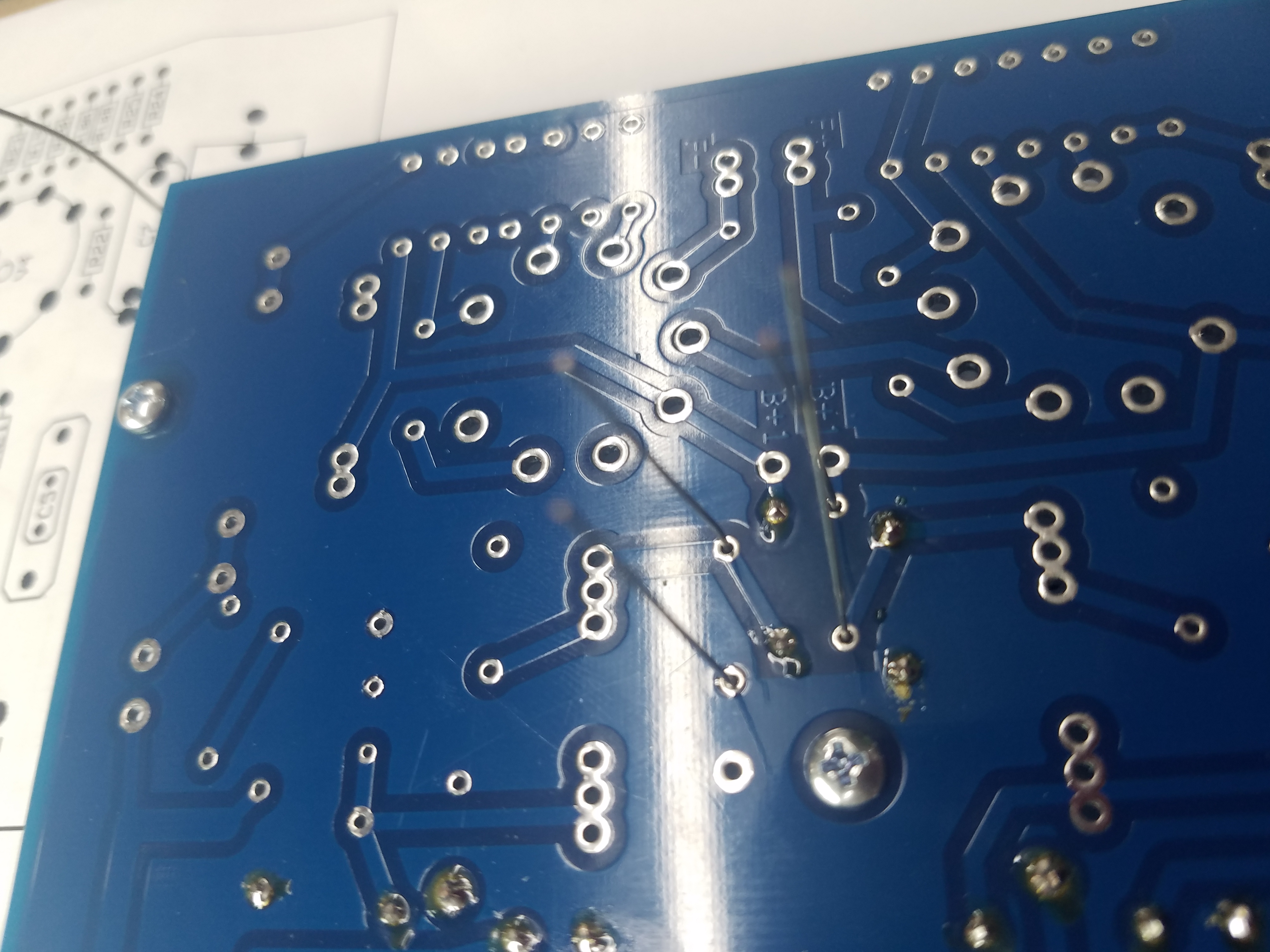
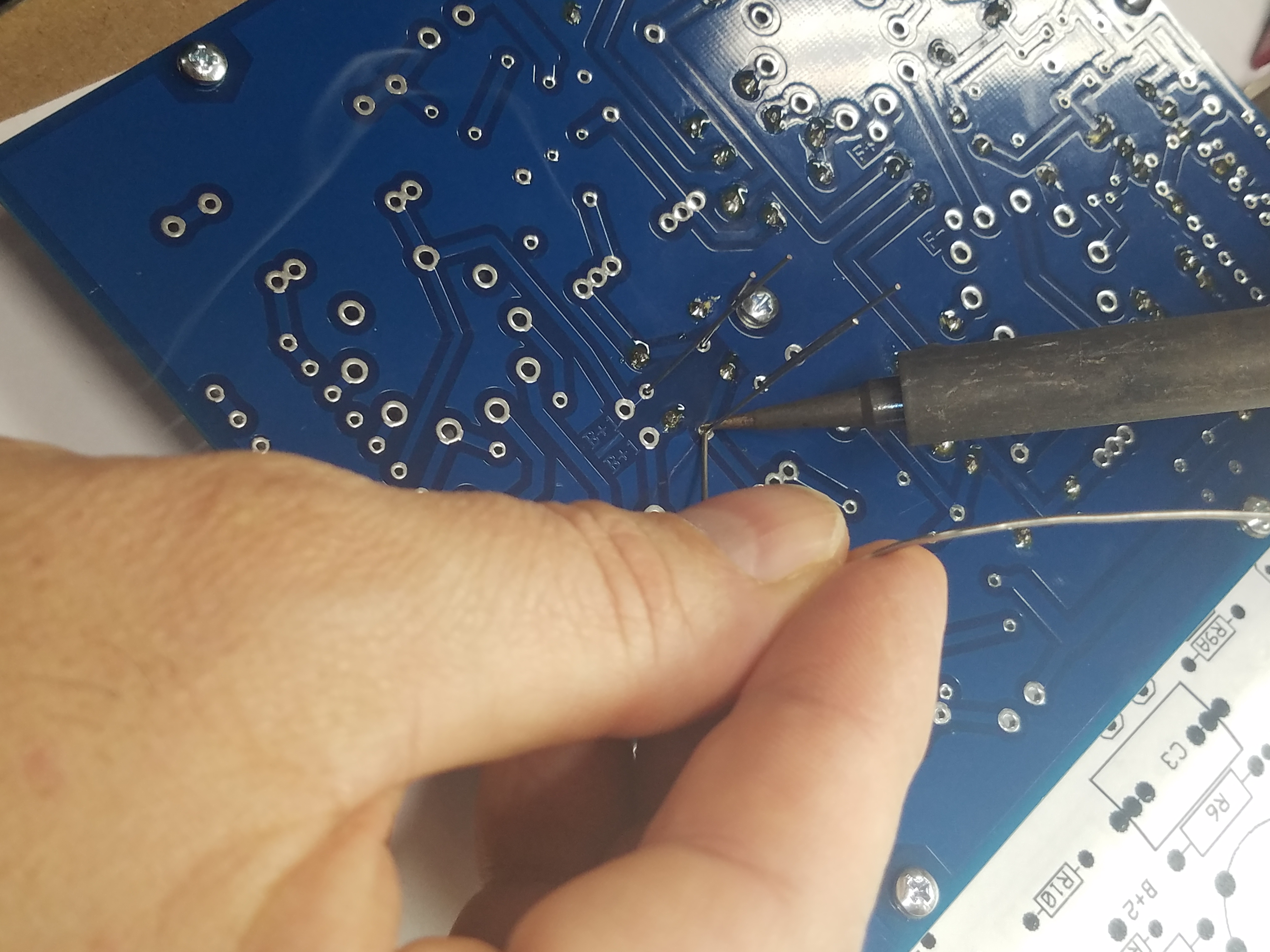
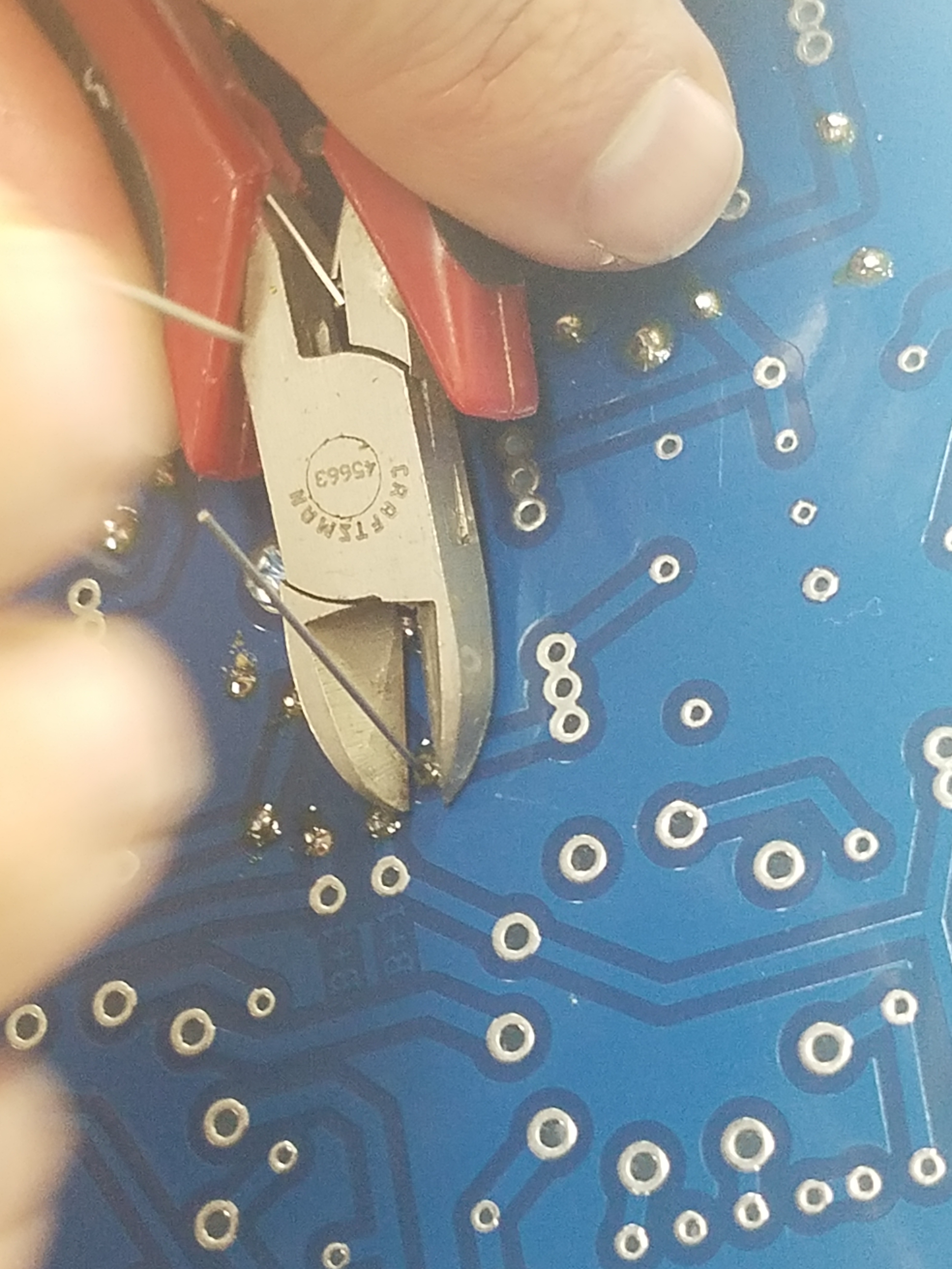
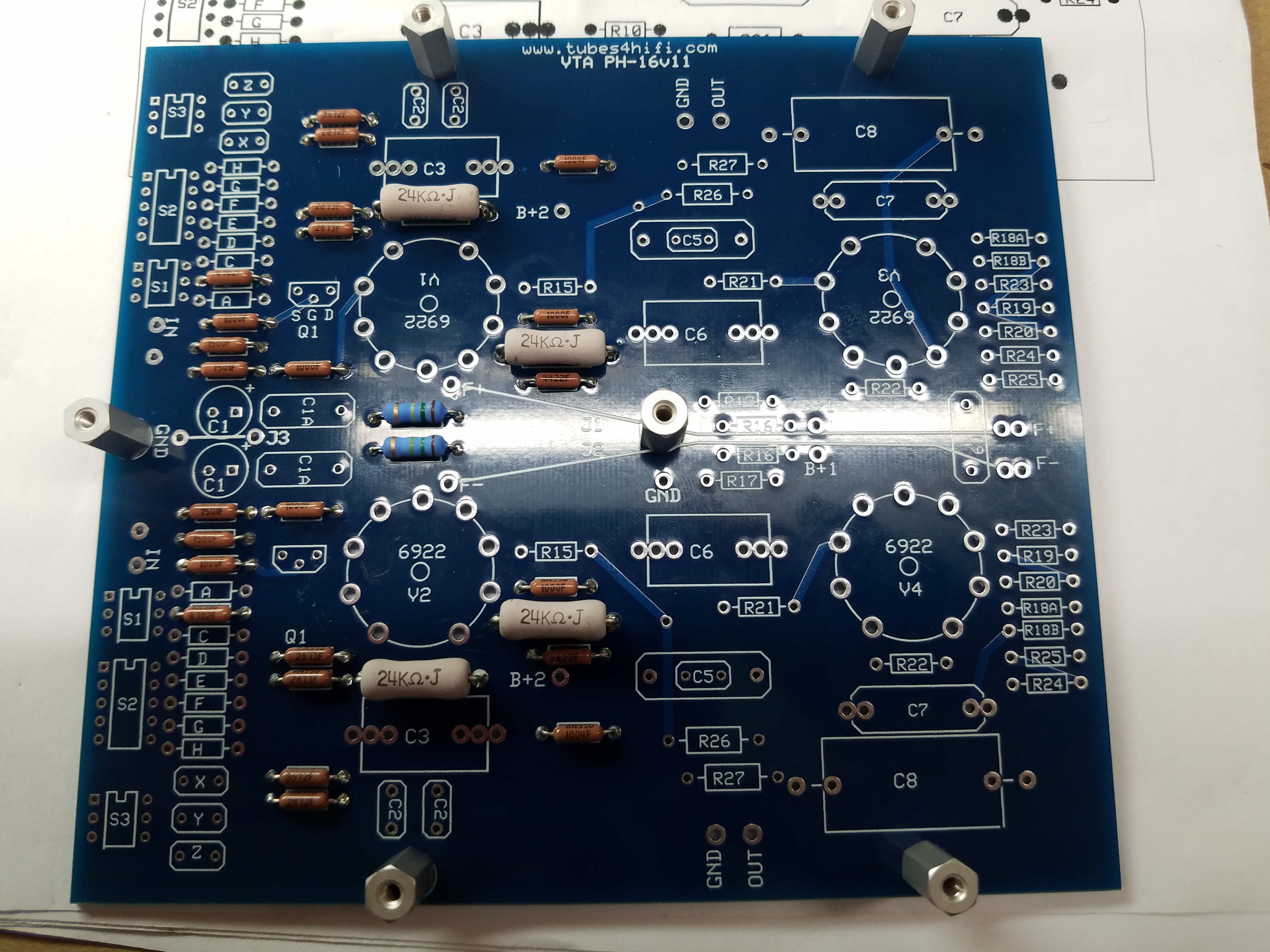
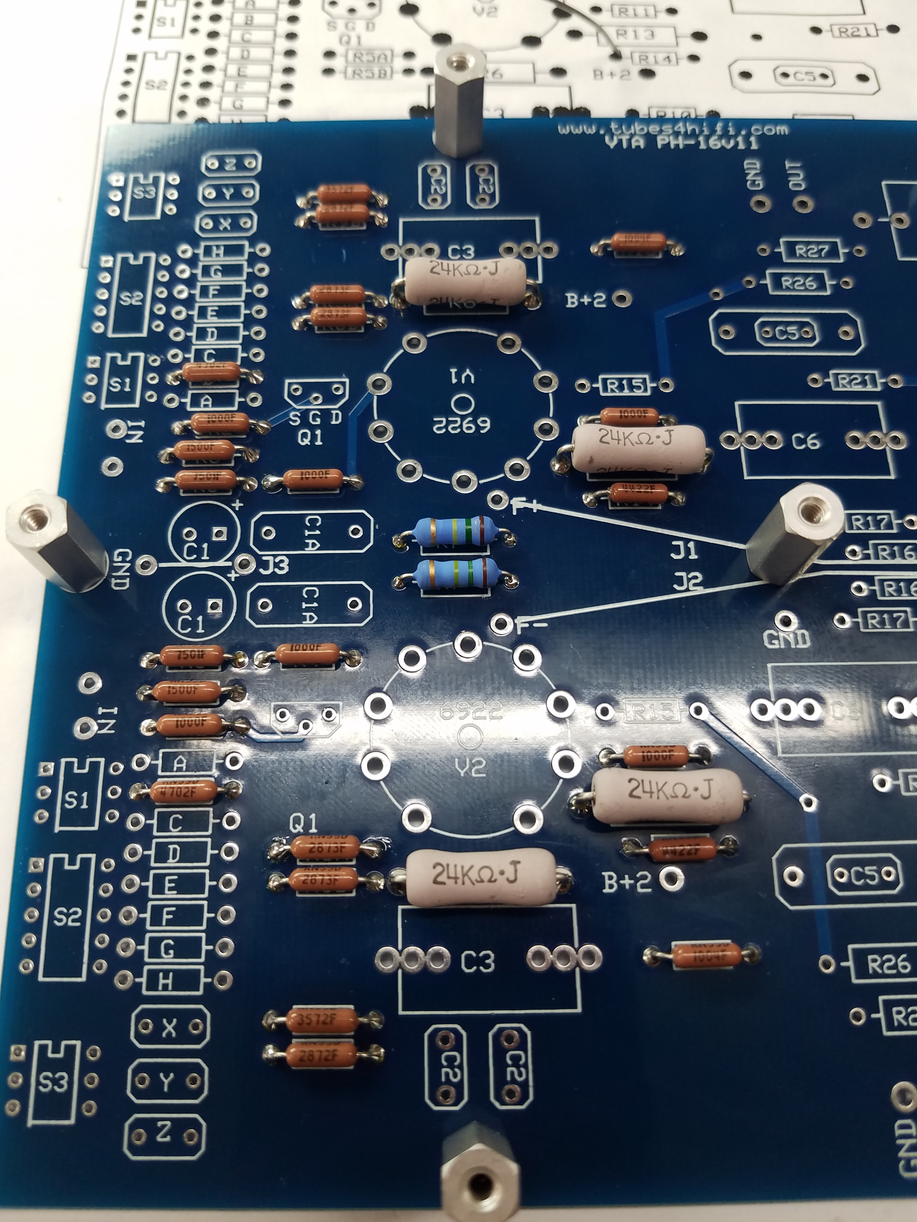
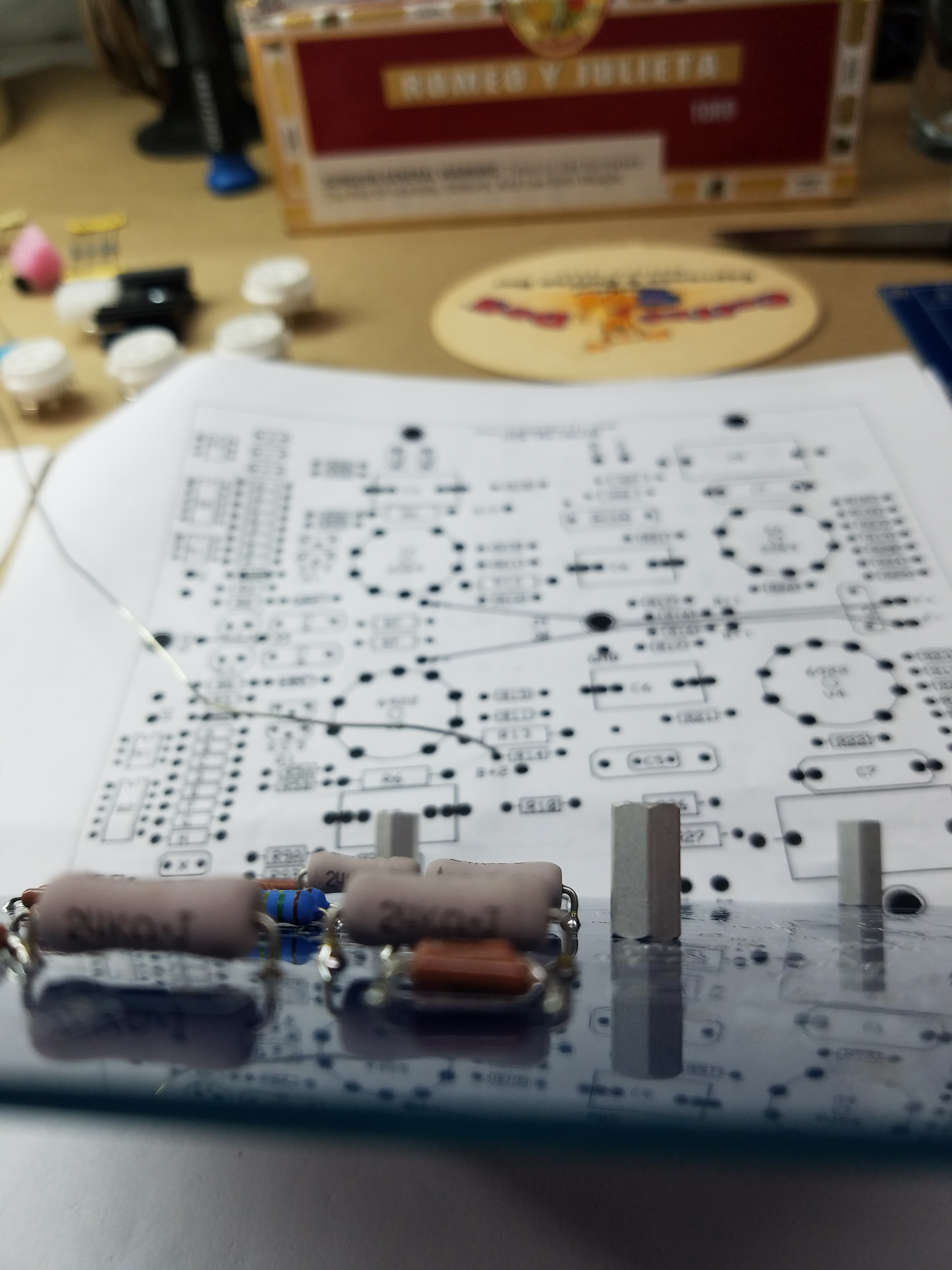
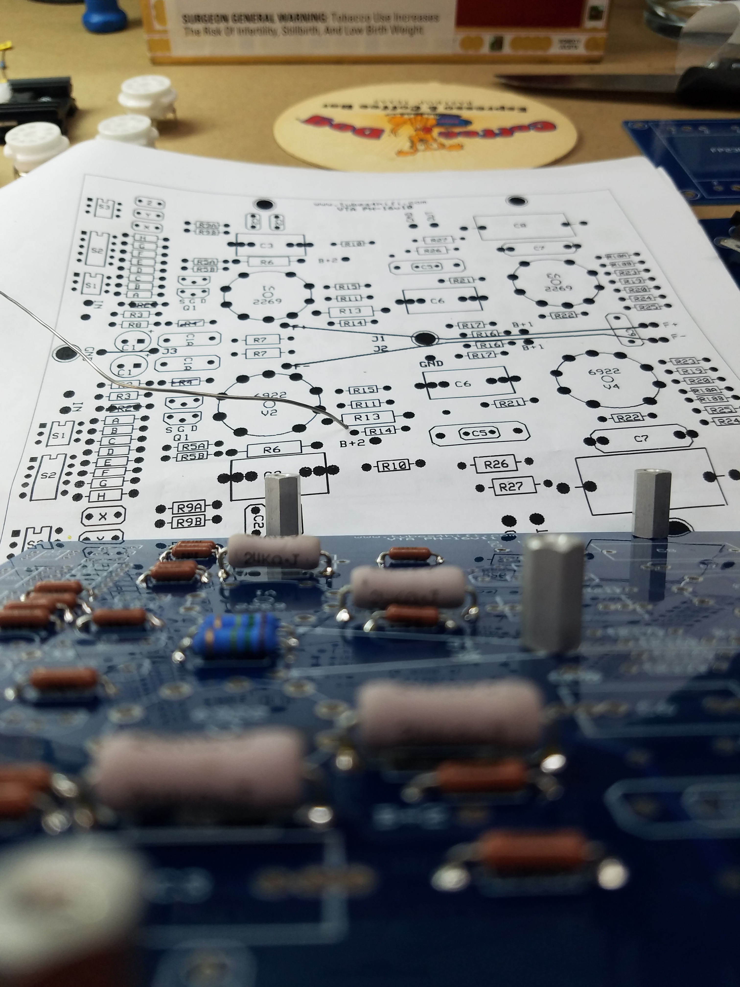
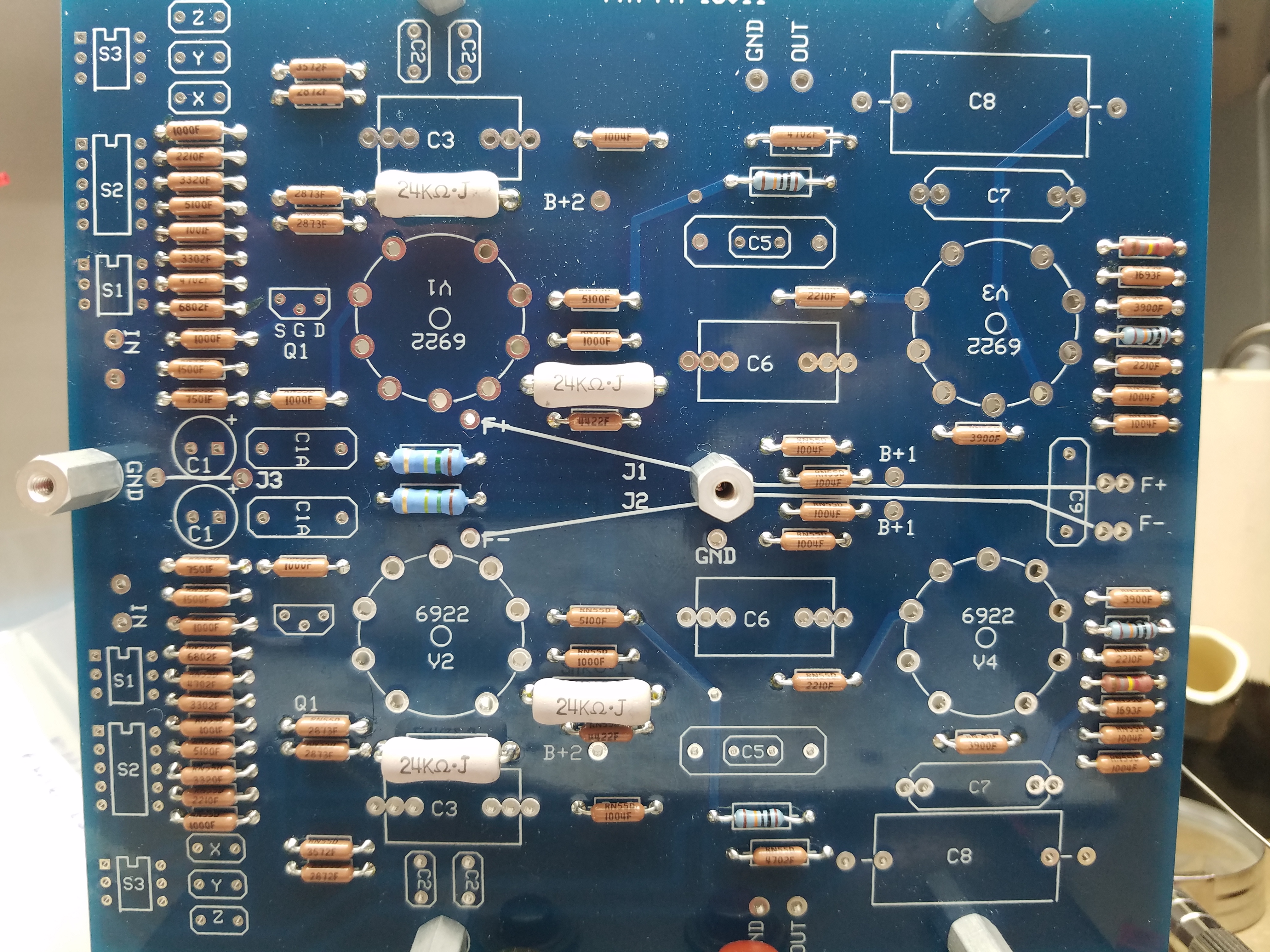
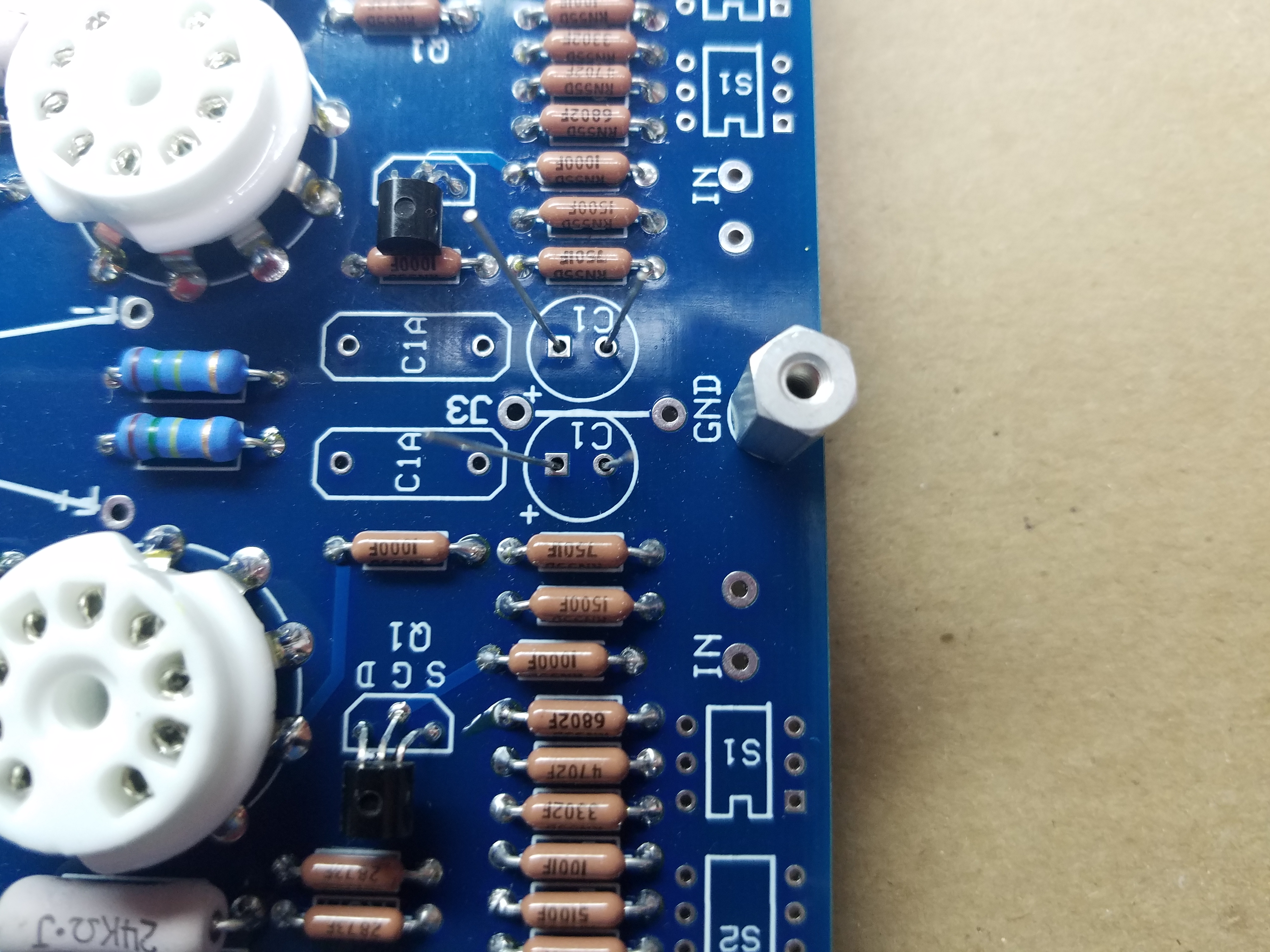
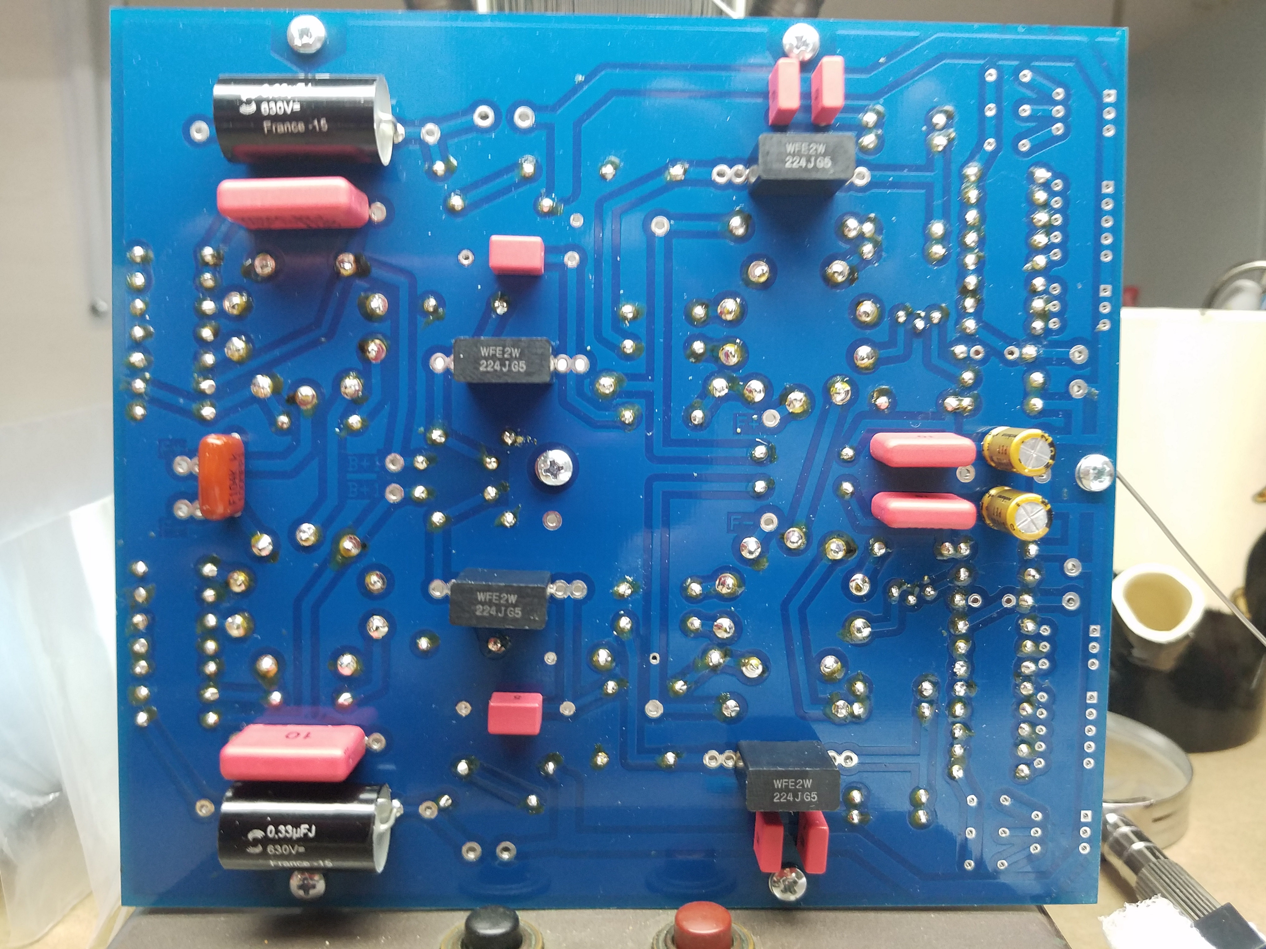
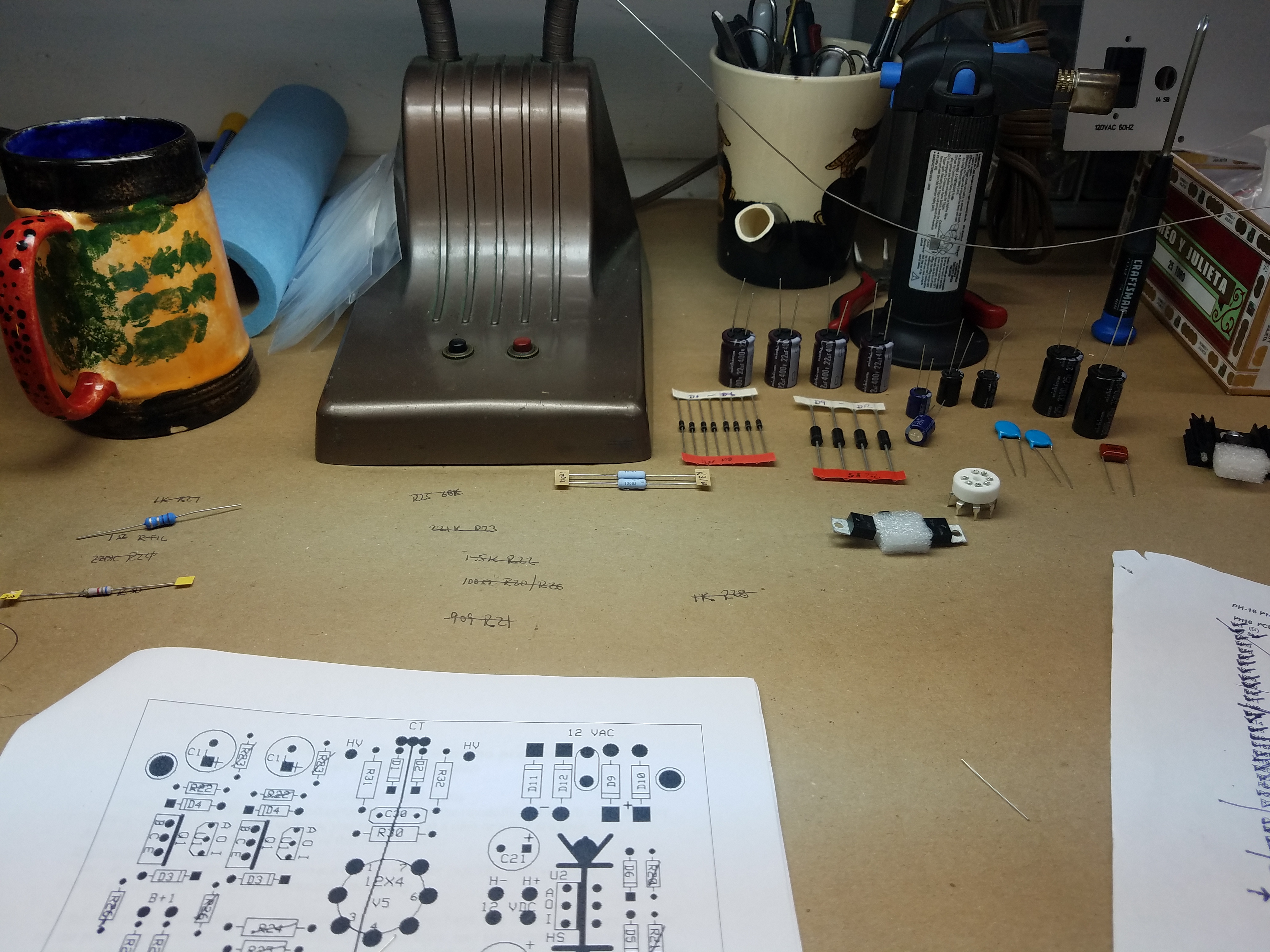
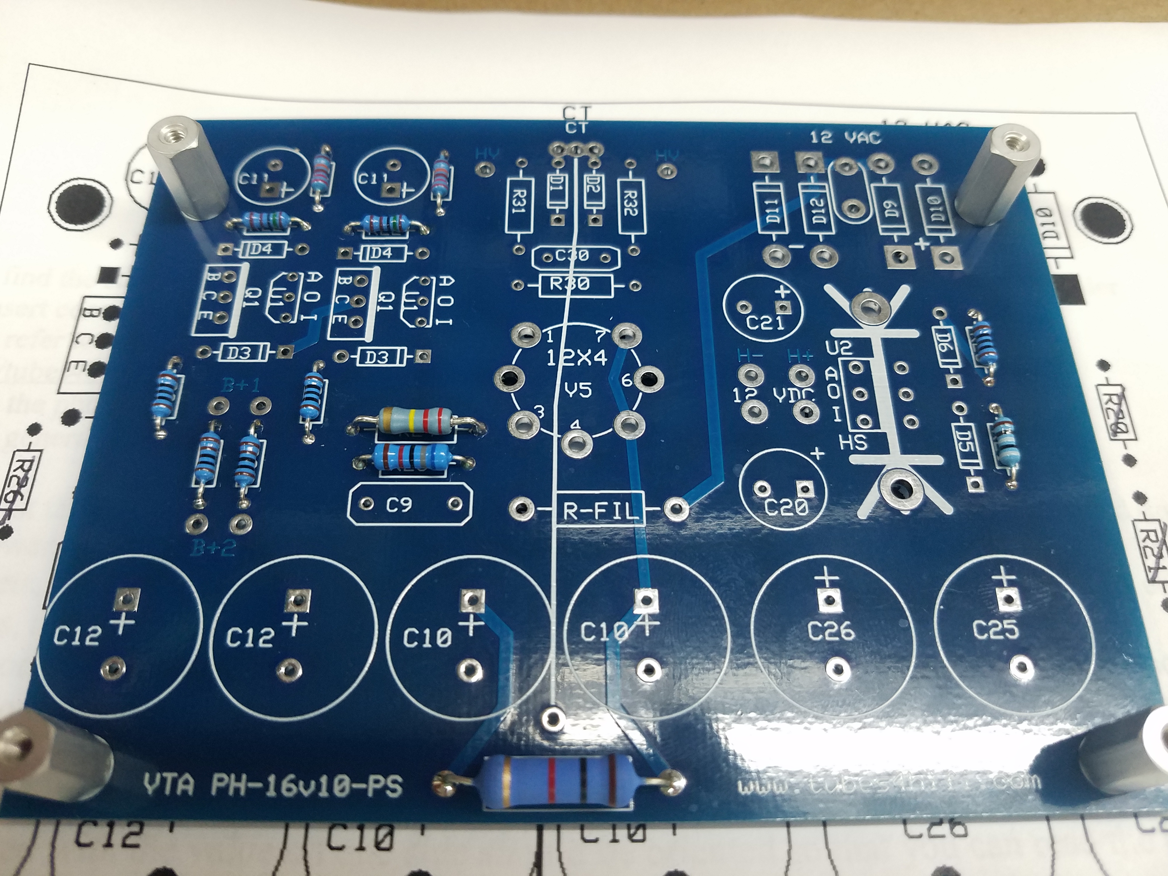
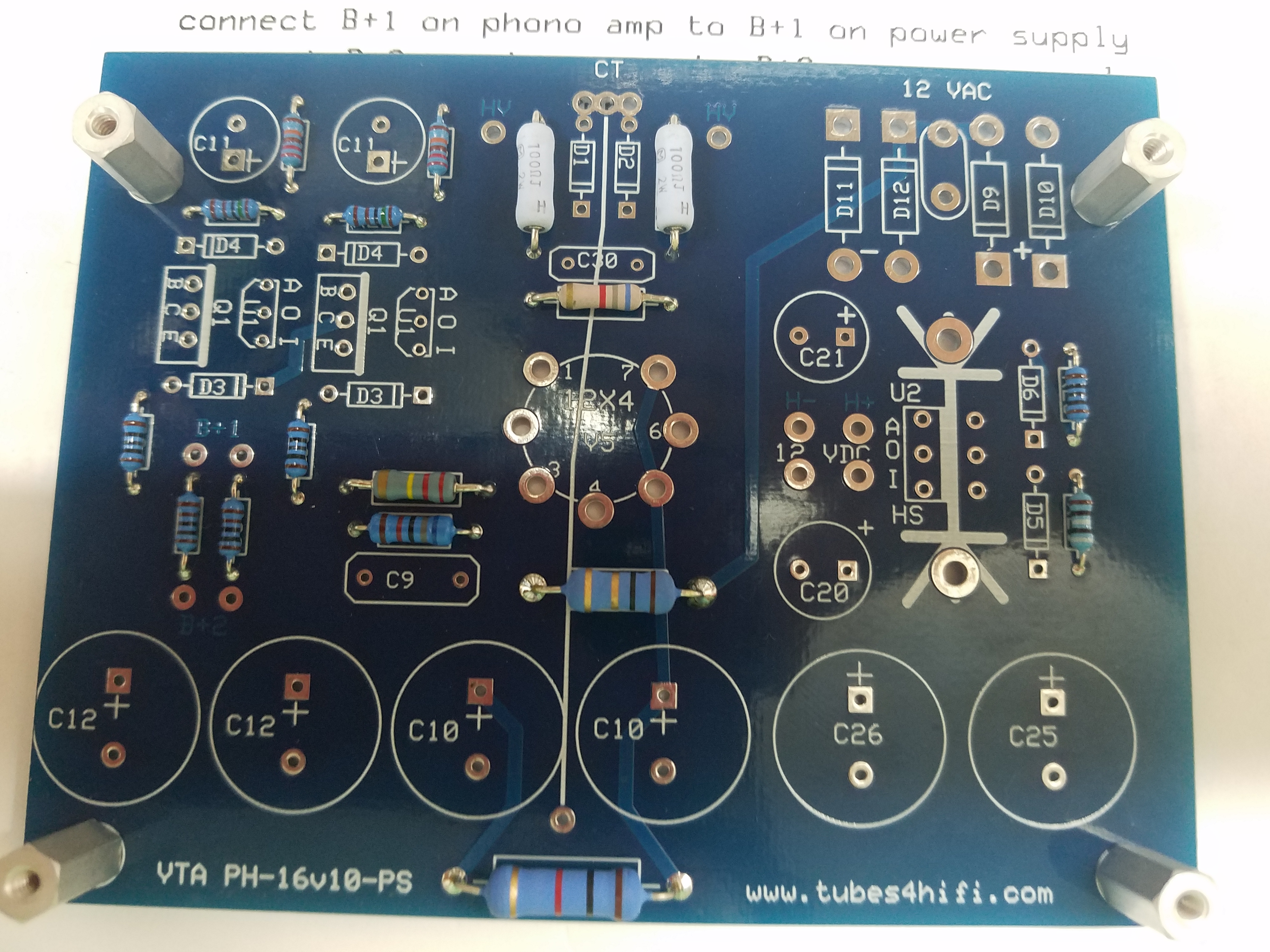
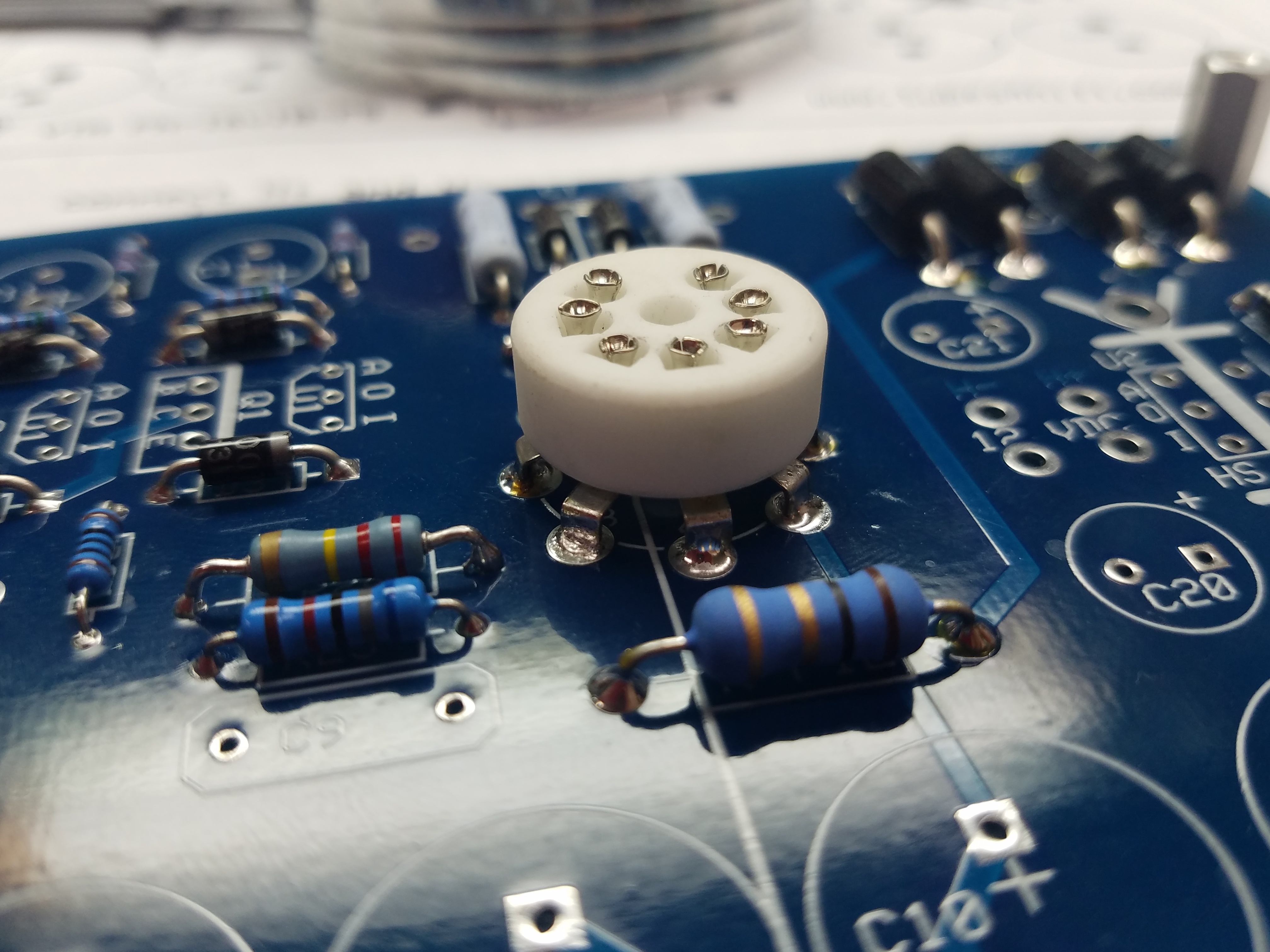
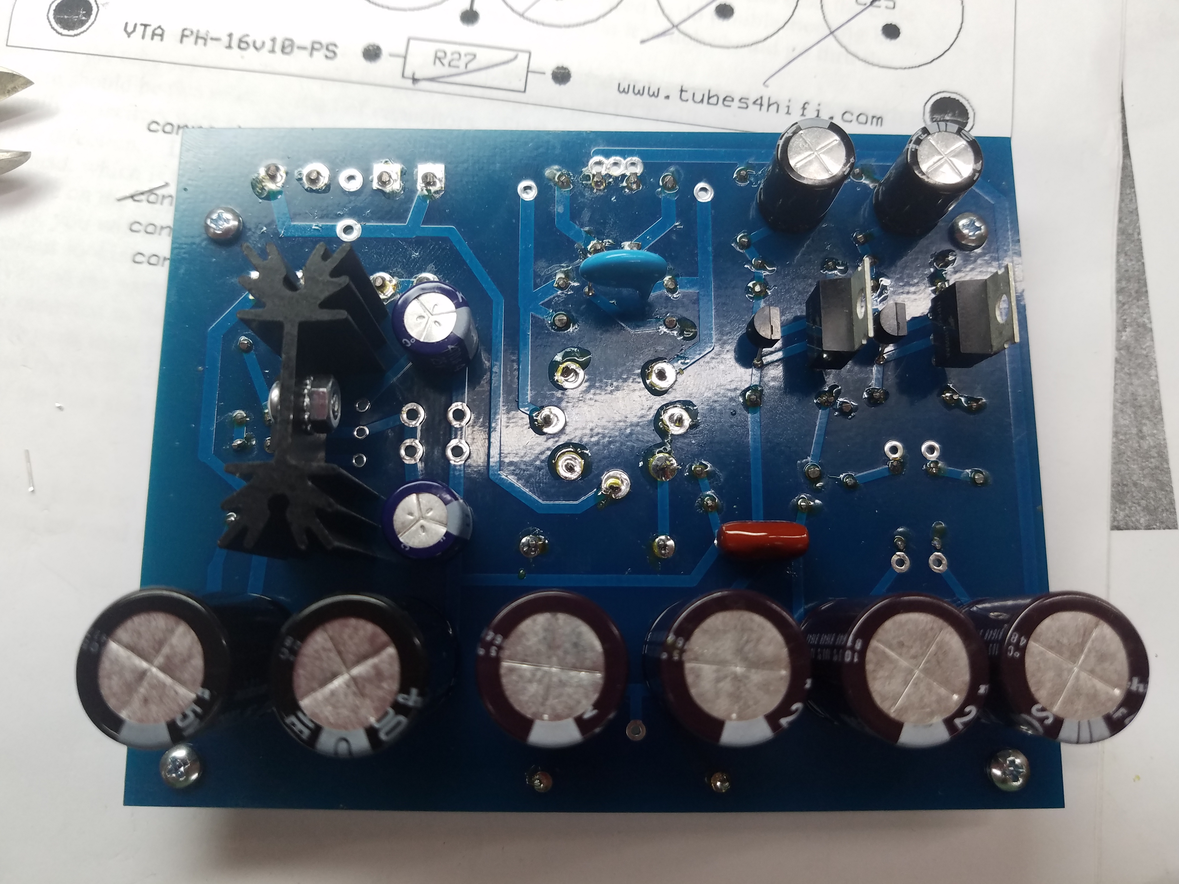
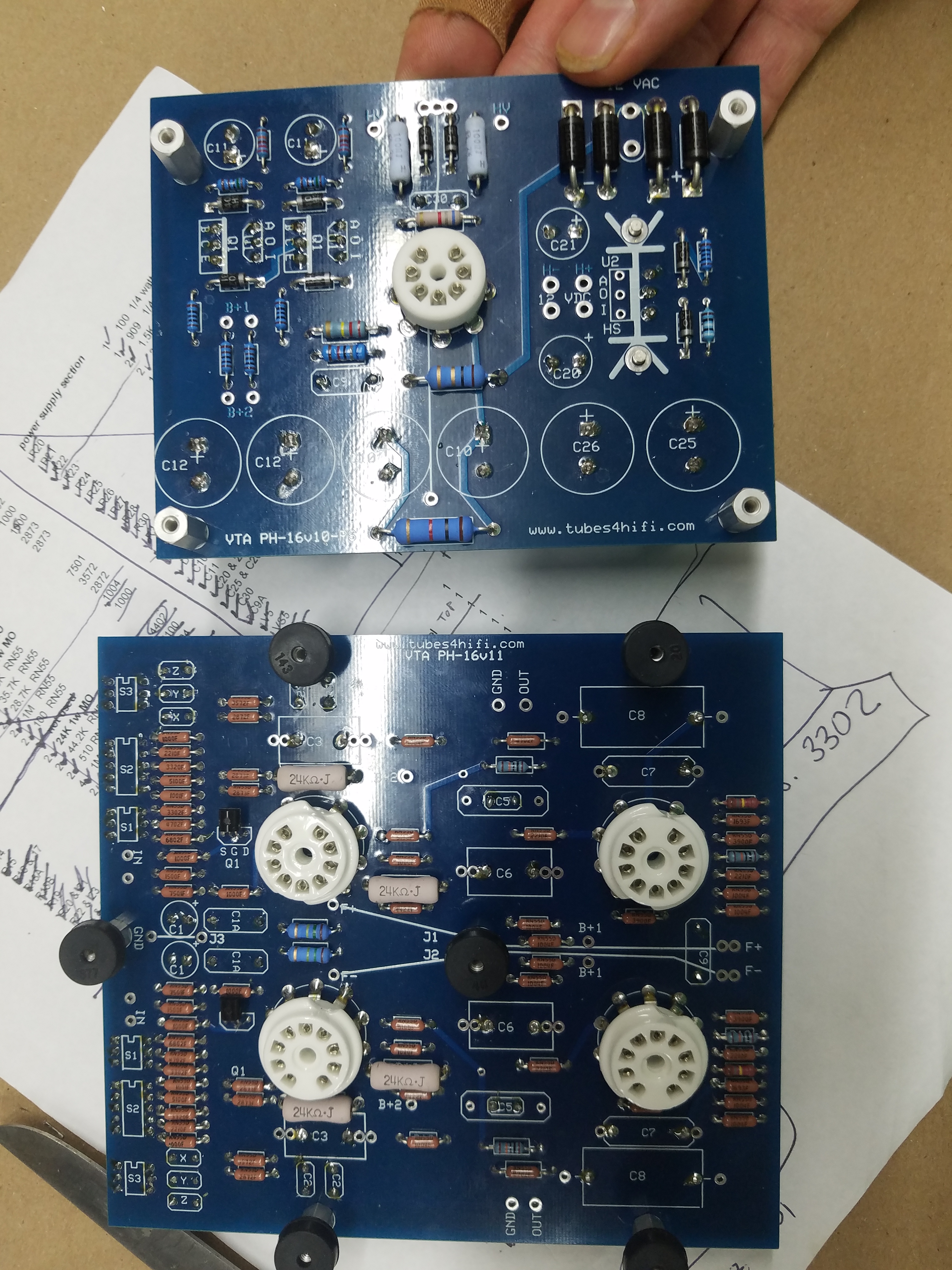
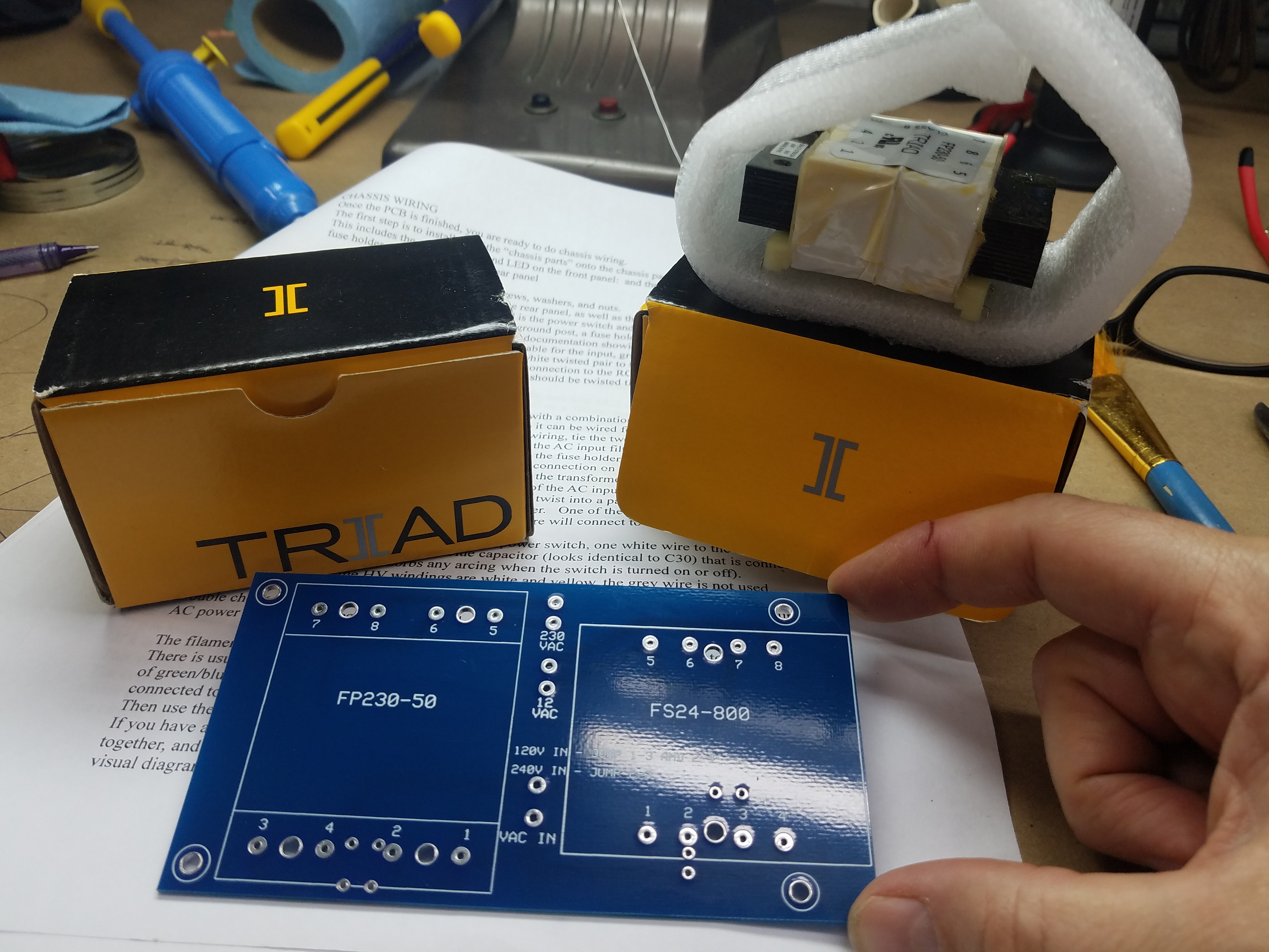
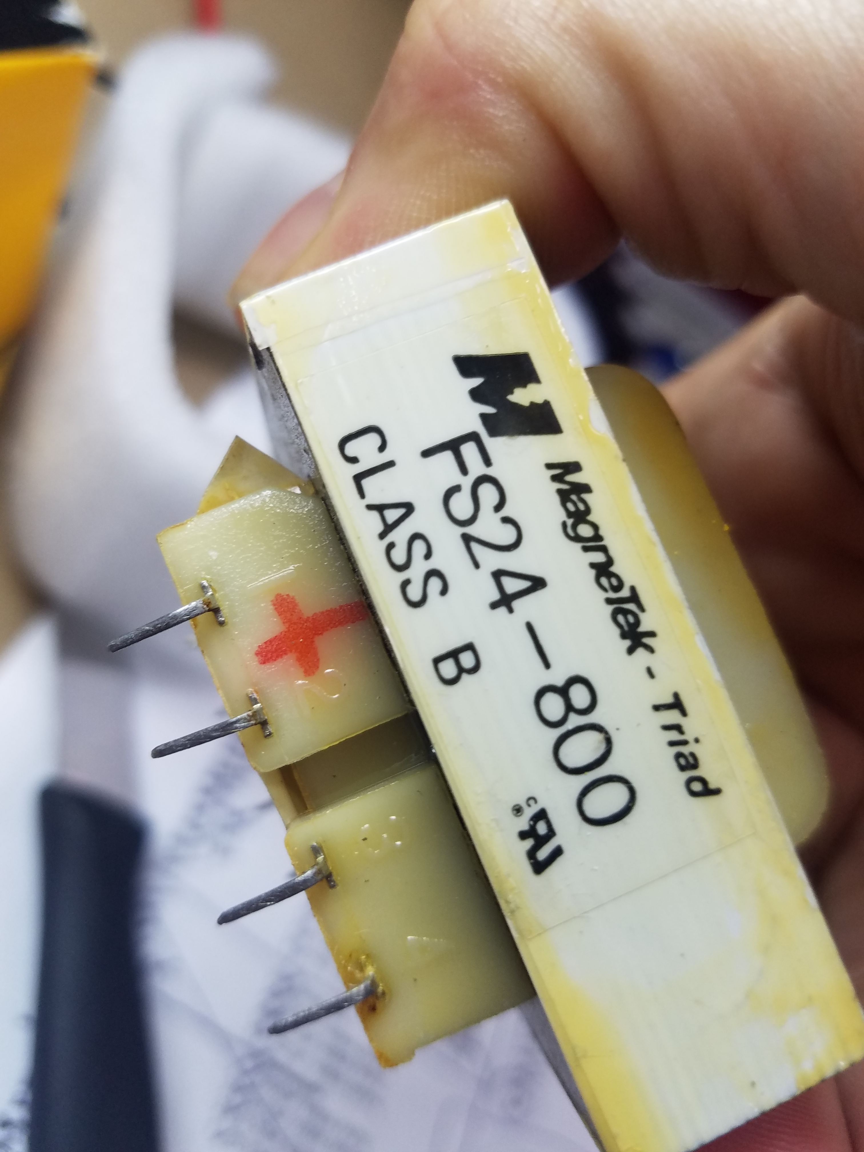
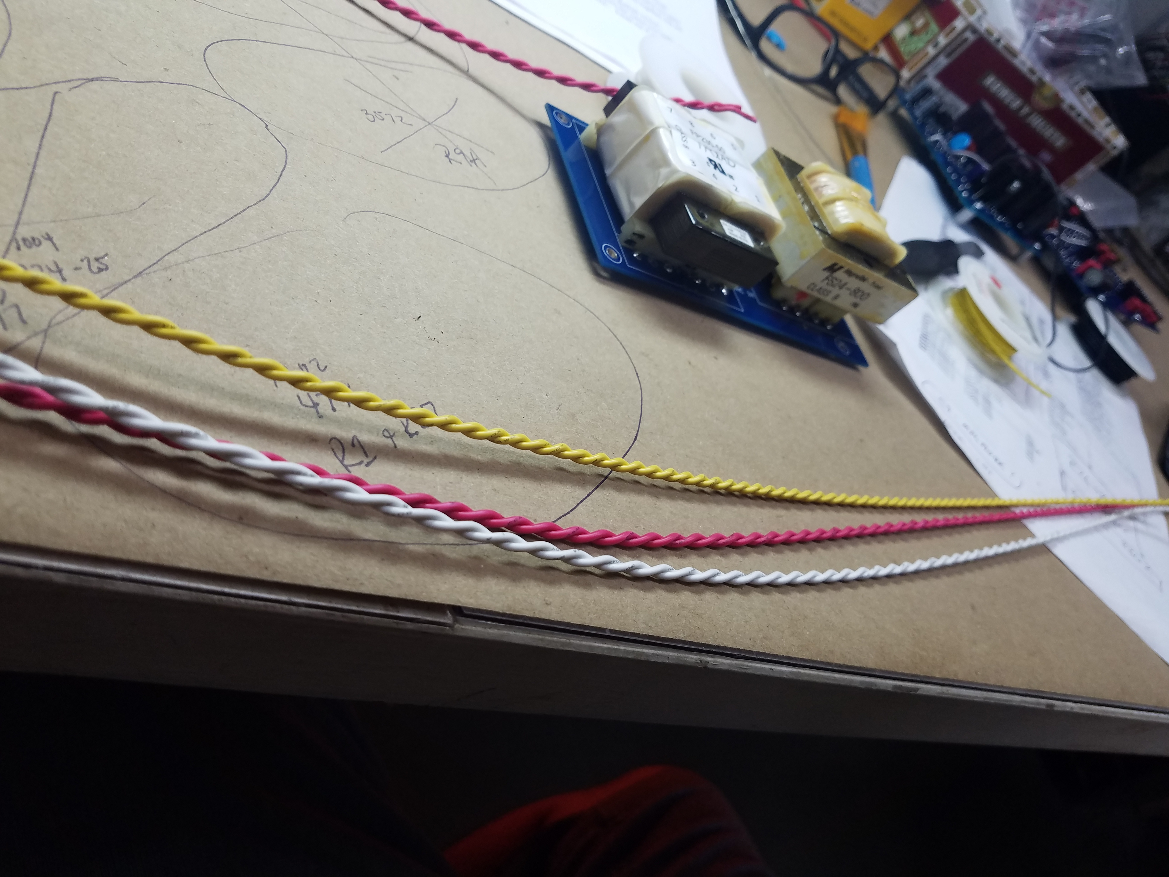
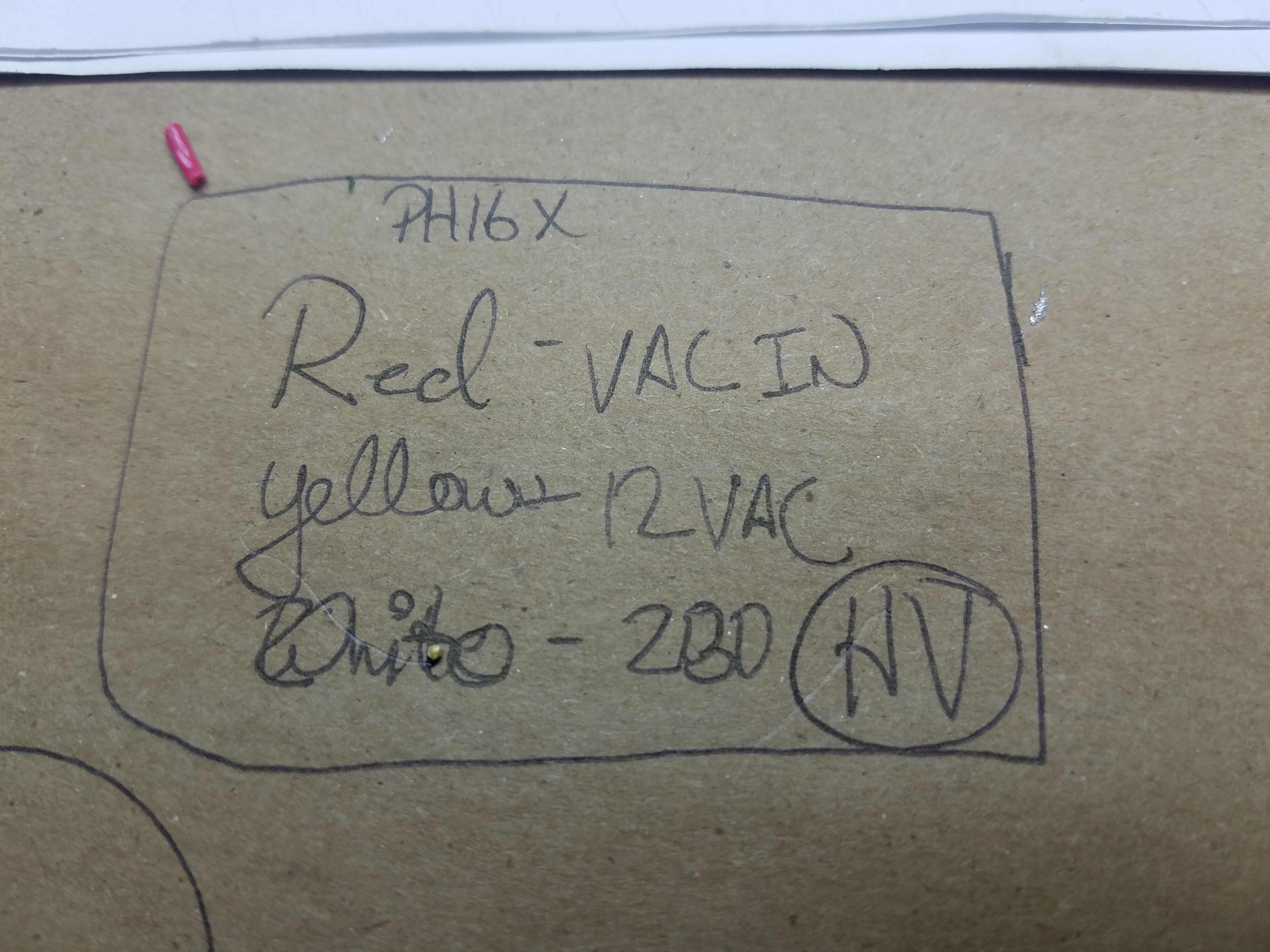
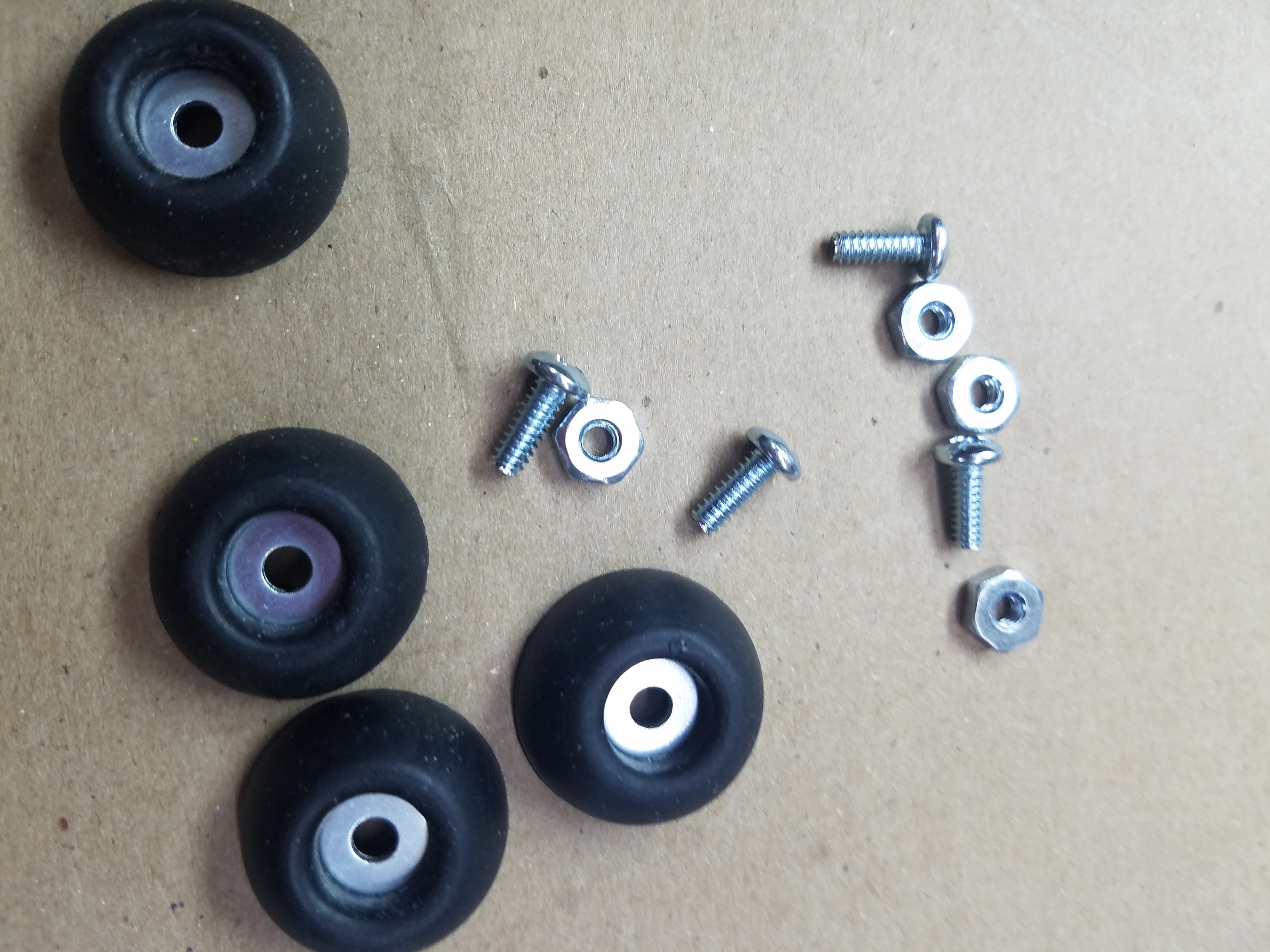
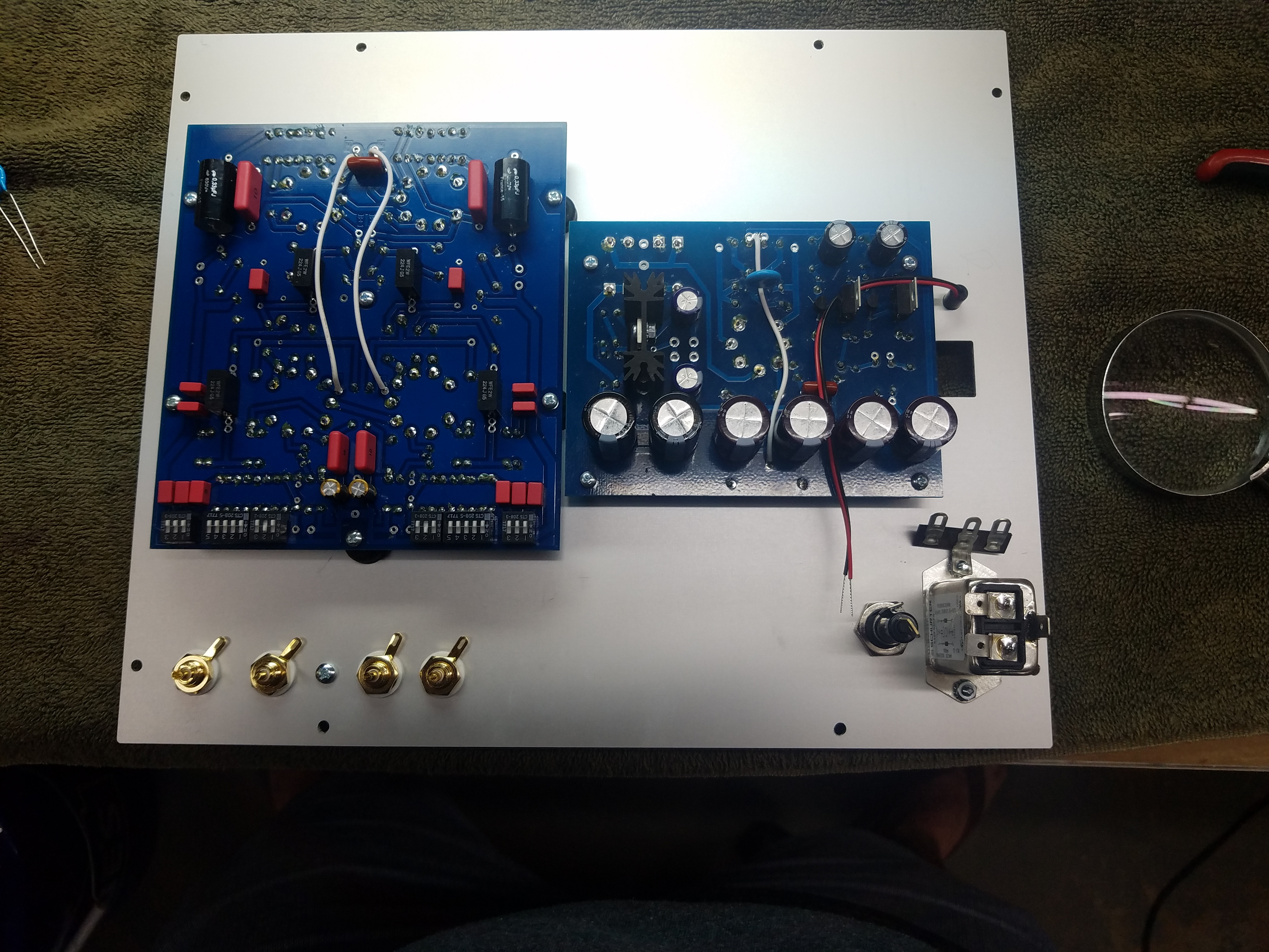
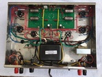
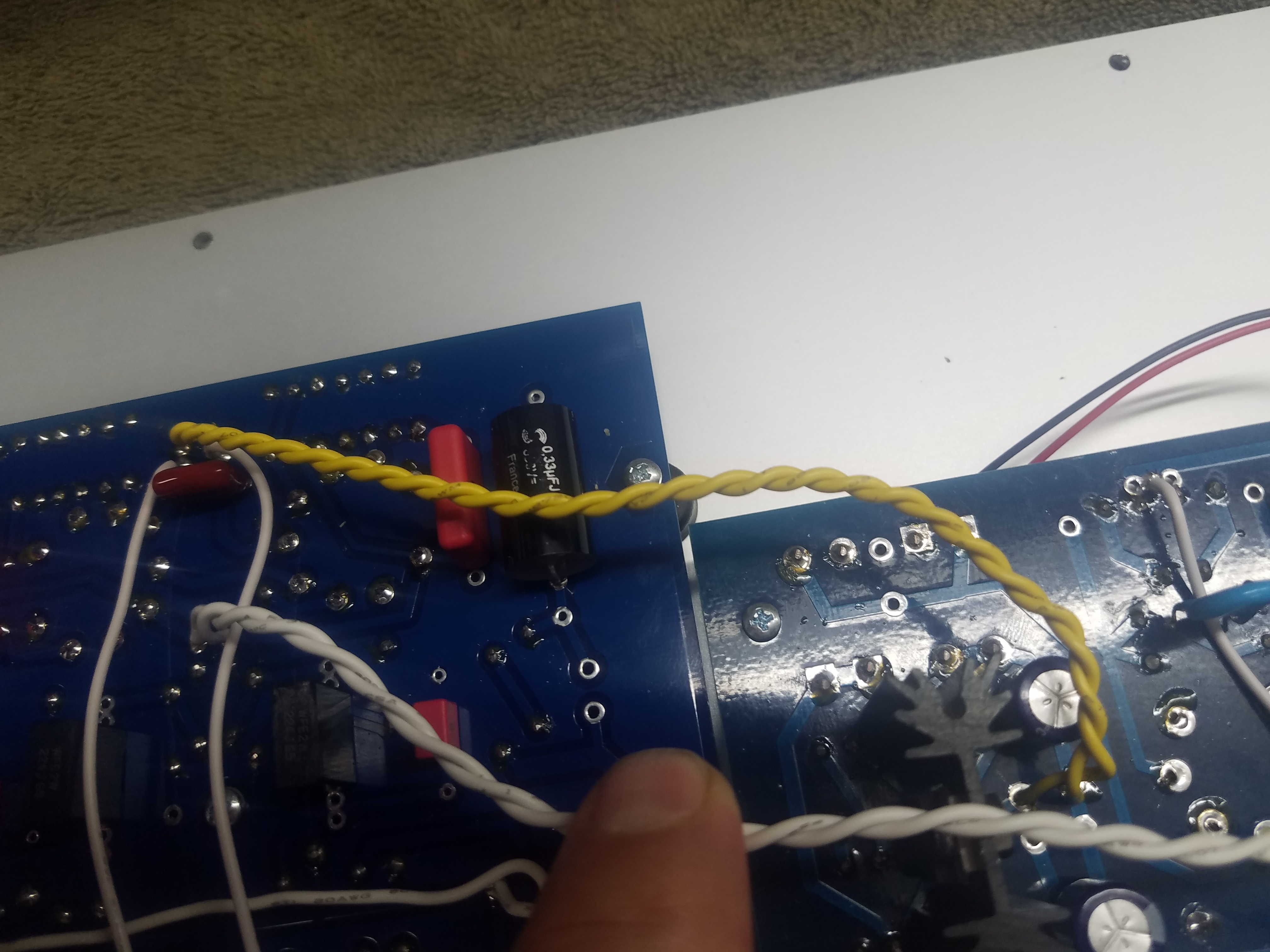
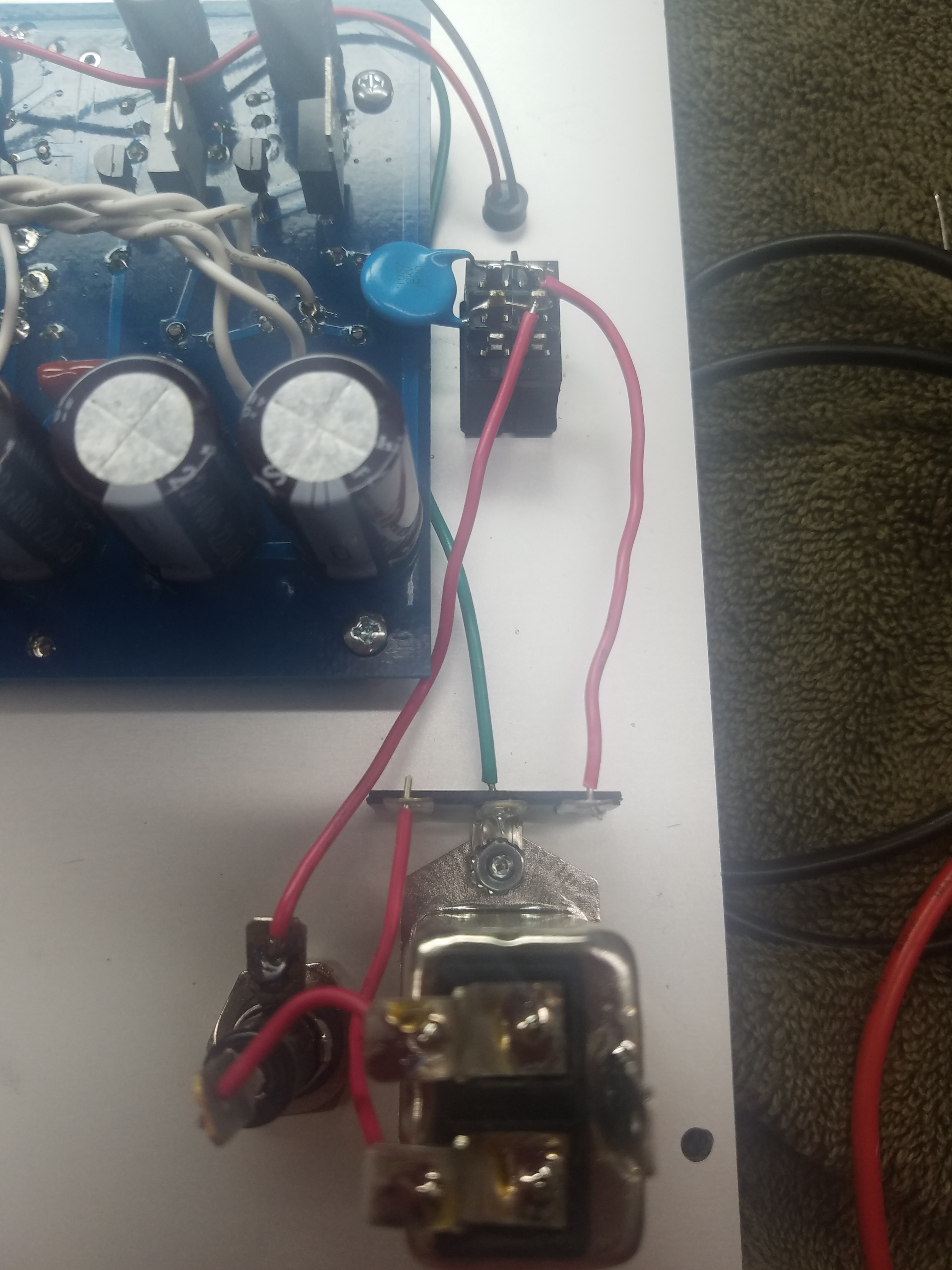
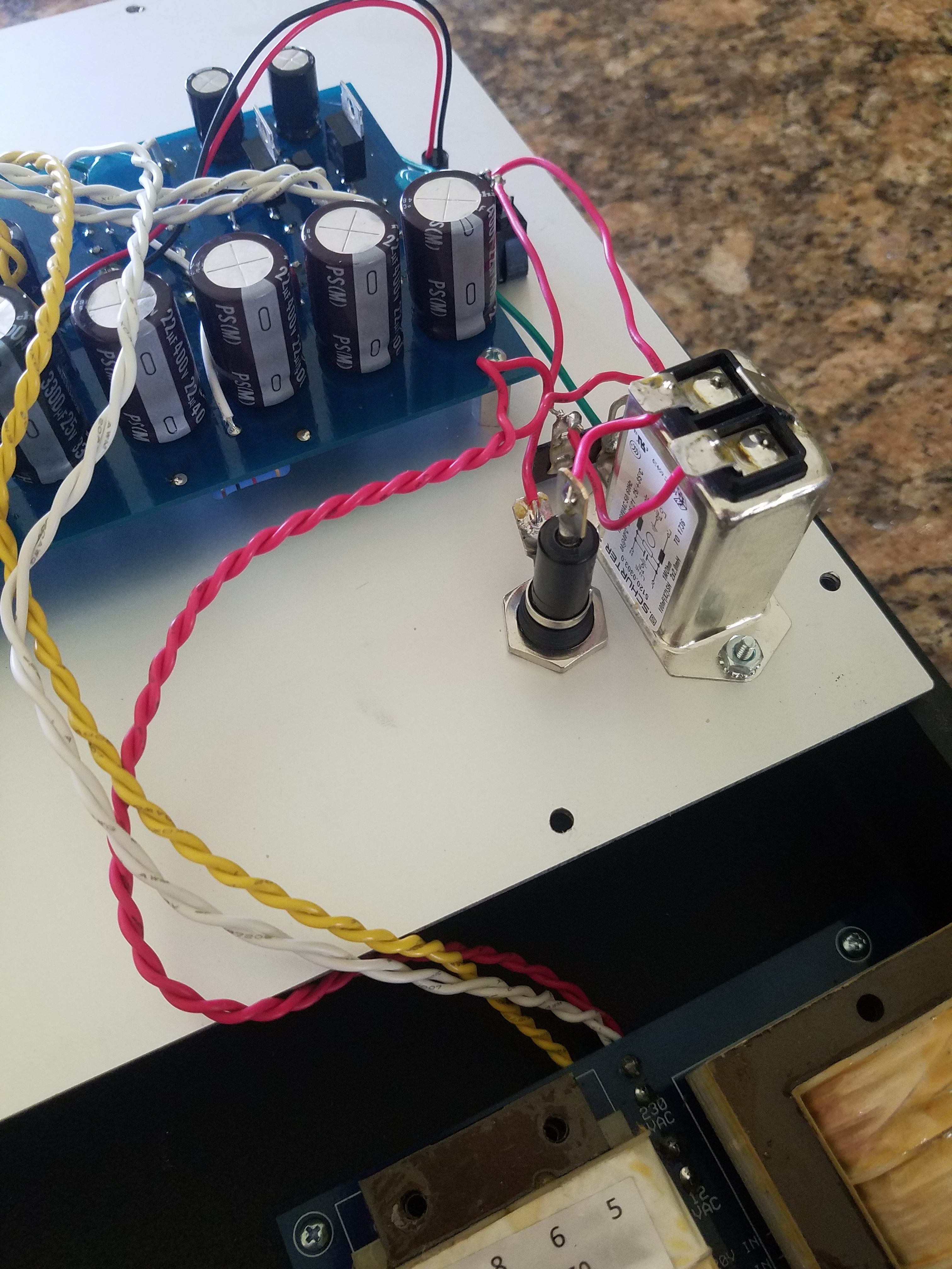
This pic is the first one after I unpacked and started to lay out all of the parts before taking inventory. (If we can see it then I'll start the discussion.)

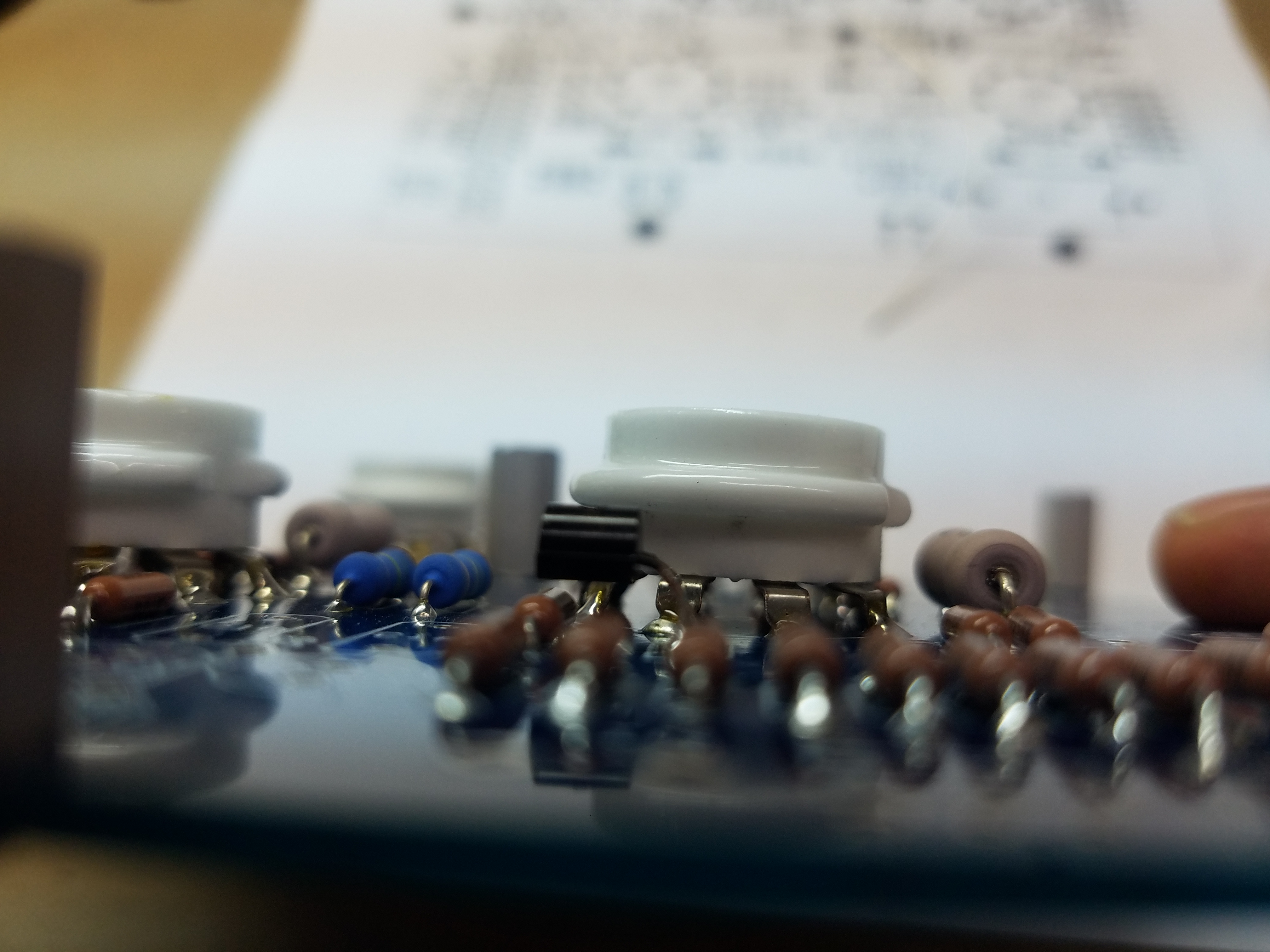
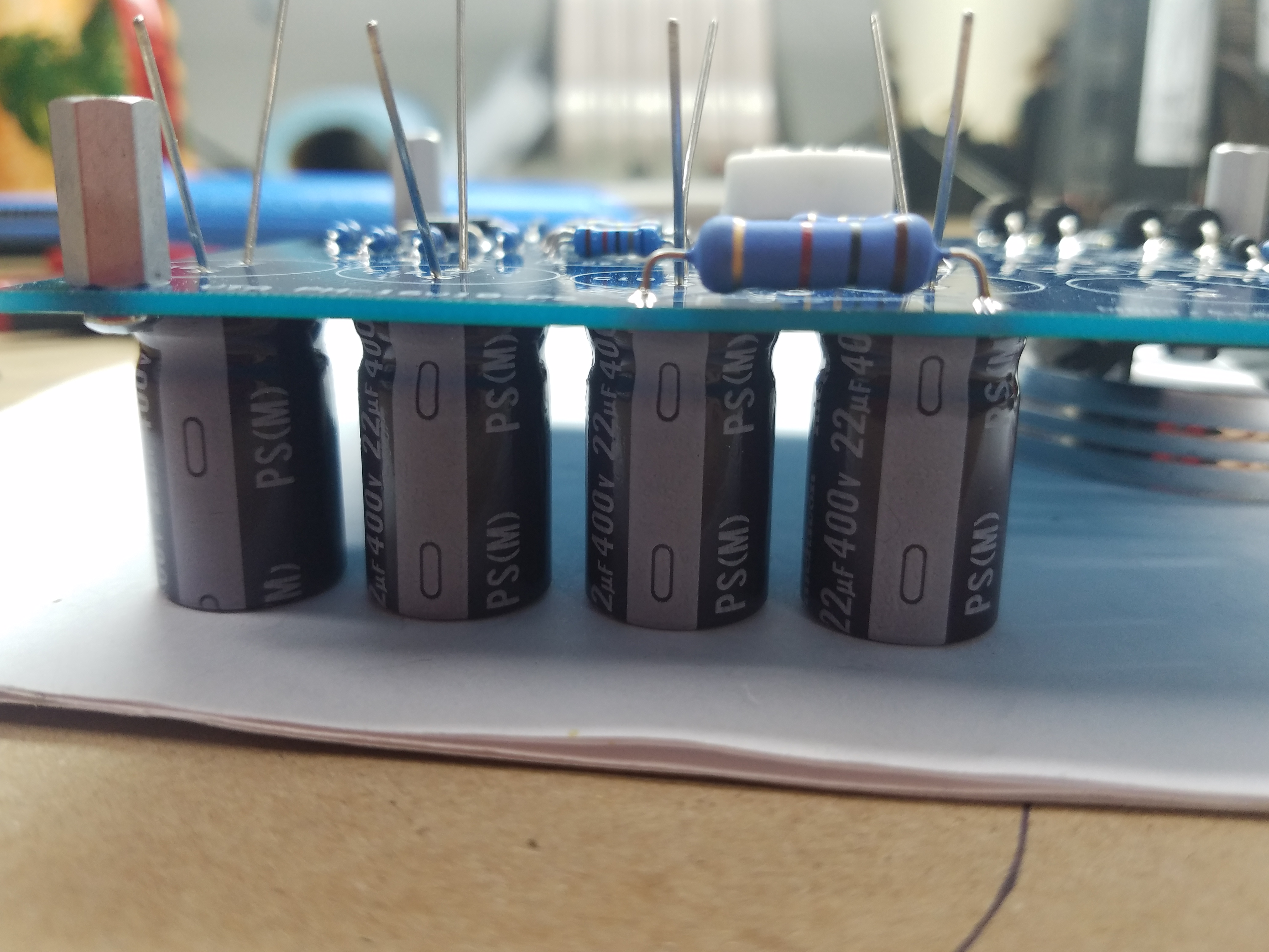
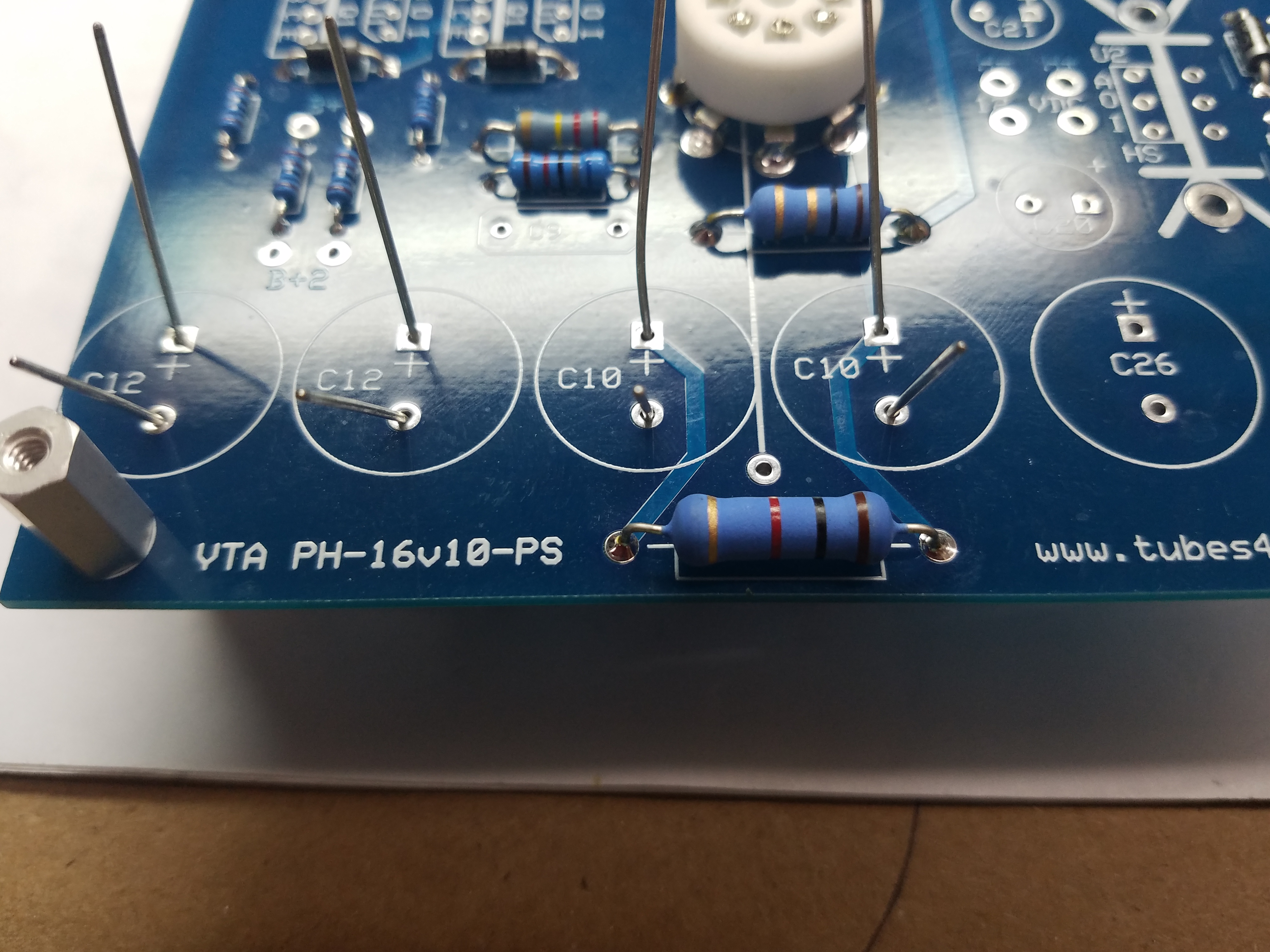
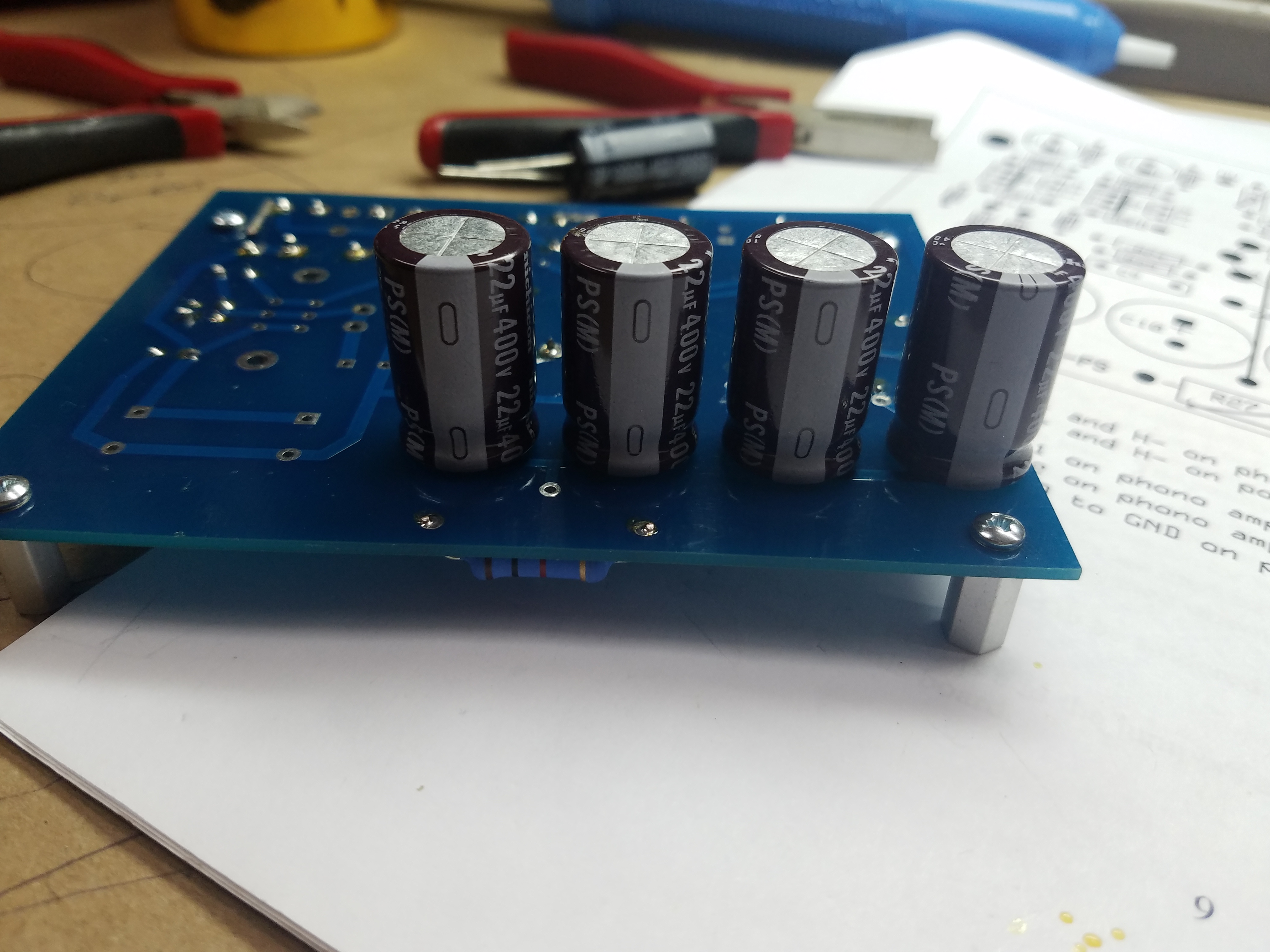
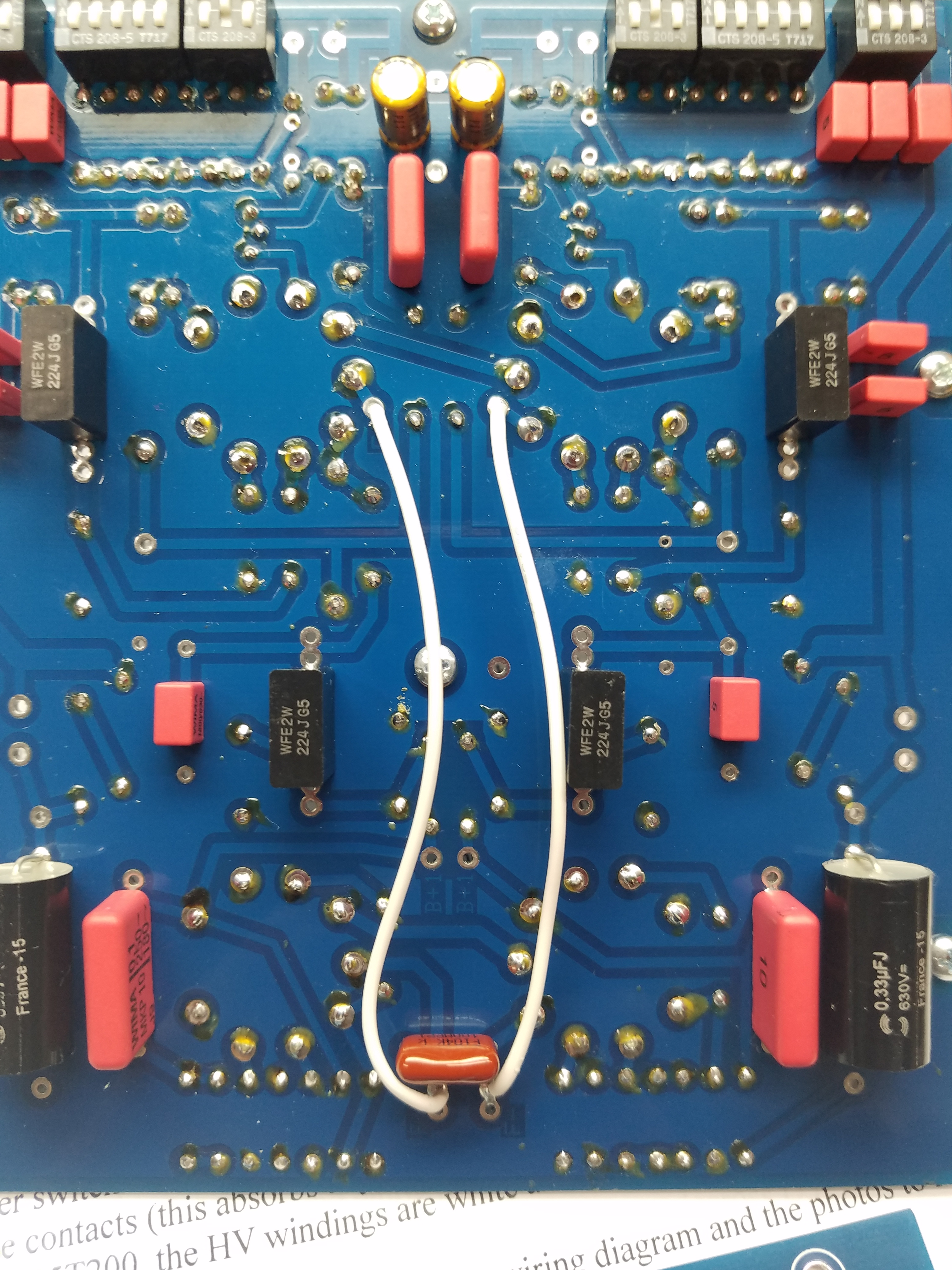
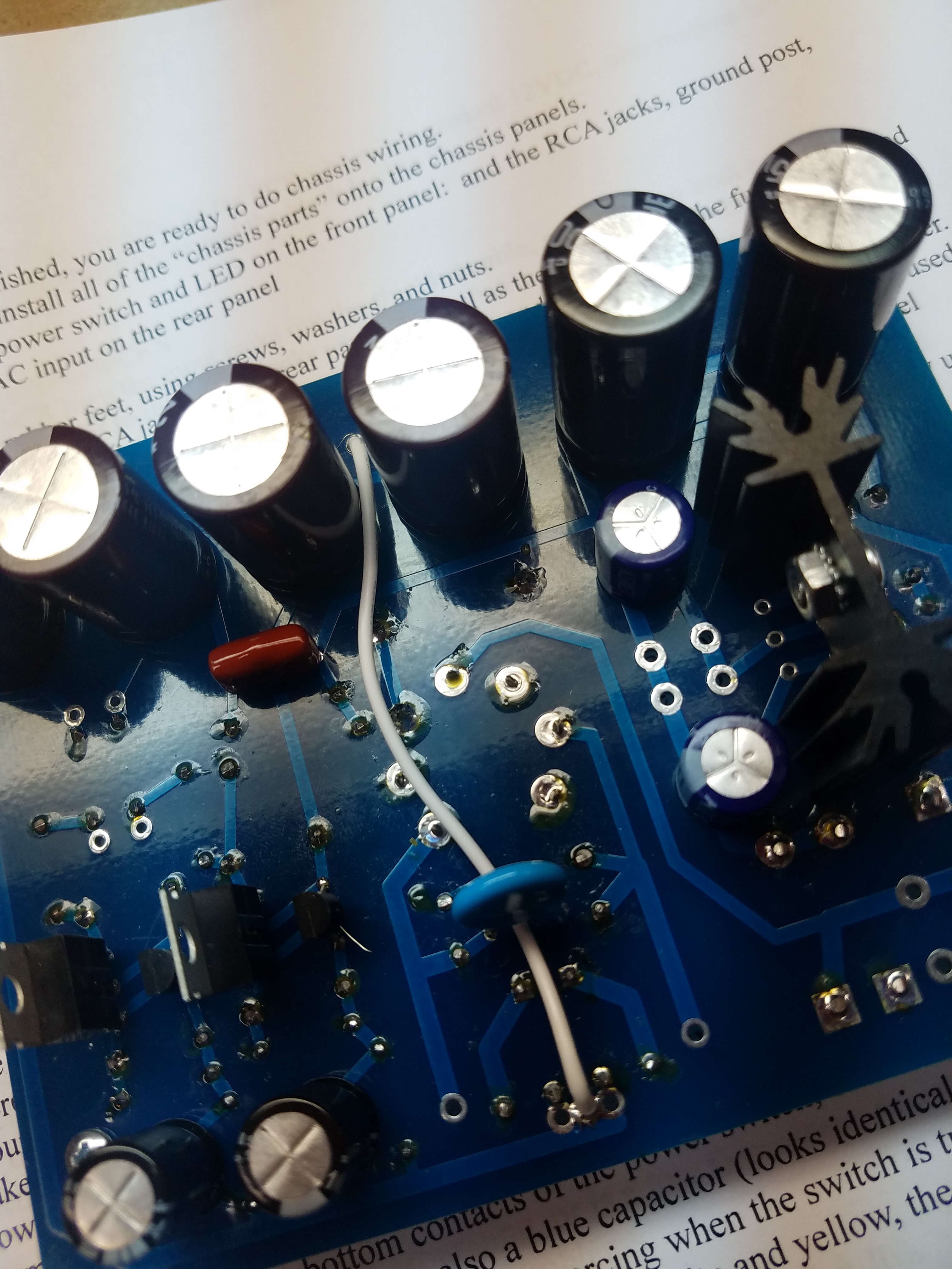
Took me a little bit, but I am closer now to having the image correct. Is it a good size or too big?
I've been a quiet member of this community for quite a while and am glad that everyone is still passionate about playing with lethal voltage for fun!
Best and more to come,
Ed in Central Texas
I would also be a fool to not mention how awesome it was to work with Kevin from Dynakit Parts too...couldn't have built my MKIIIs without him.
It was 7 years ago that I built my VTA SP12 with a PH12 included. It was one of the very first SP12 kits that Roy sold (possibly even the first SP12 not built by Roy, but I'm not entirely sure.) I had just added to VTA board to my Dynaco ST70, and knew I needed to get into Roy's other designs. Both Roy and Bob were great help as I dove into this hobby all those years ago, and they never fail to be a great resource when their help is needed. I would also be a fool to not mention how awesome it was to work with Kevin from Dynakit Parts too...couldn't have built my MKIIIs without him.
I've since built my own set of speakers, a design by Paul Carmody called 'Sunflowers.' They sound great! I then built a nixie tube chessboard lit by induction coils designed by Tony 'Lasermad' Adams from the UK, and I've completely rebuilt a set of Dynaco MKIII Monoblocks, adding Roy's driver board to them with octal 6SN7s. I also followed my tube obsession into amateur radio and became a ham a couple of years ago...so 73 from W8EFG.
So........My birthday happened last weekend and my wife contacted Roy and bought me the PCB kit for the PH16X. AND she gave me permission to buy the rest of it as well as to squeeze in an SP14 kit too. Best birthday ever!!!
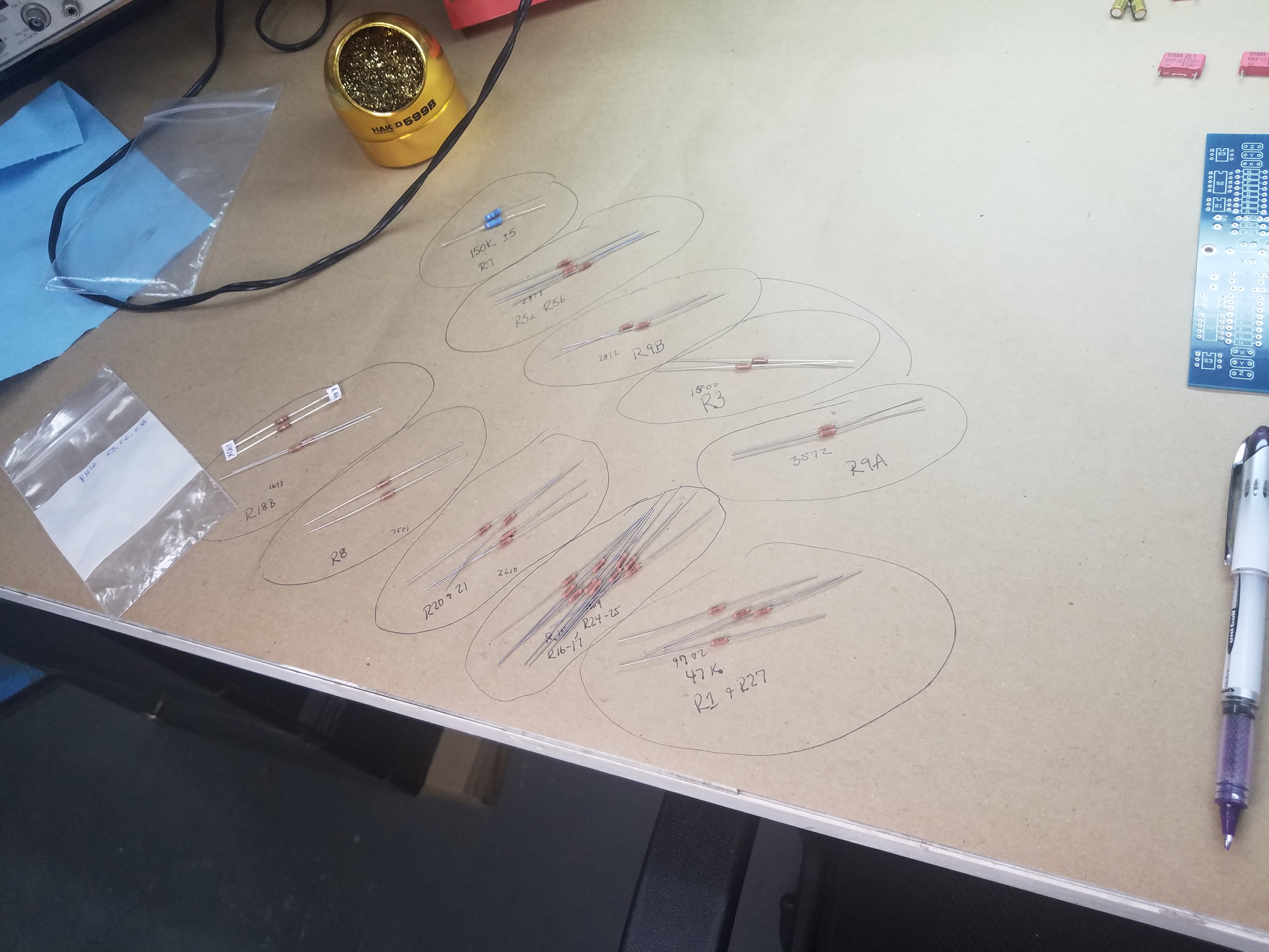
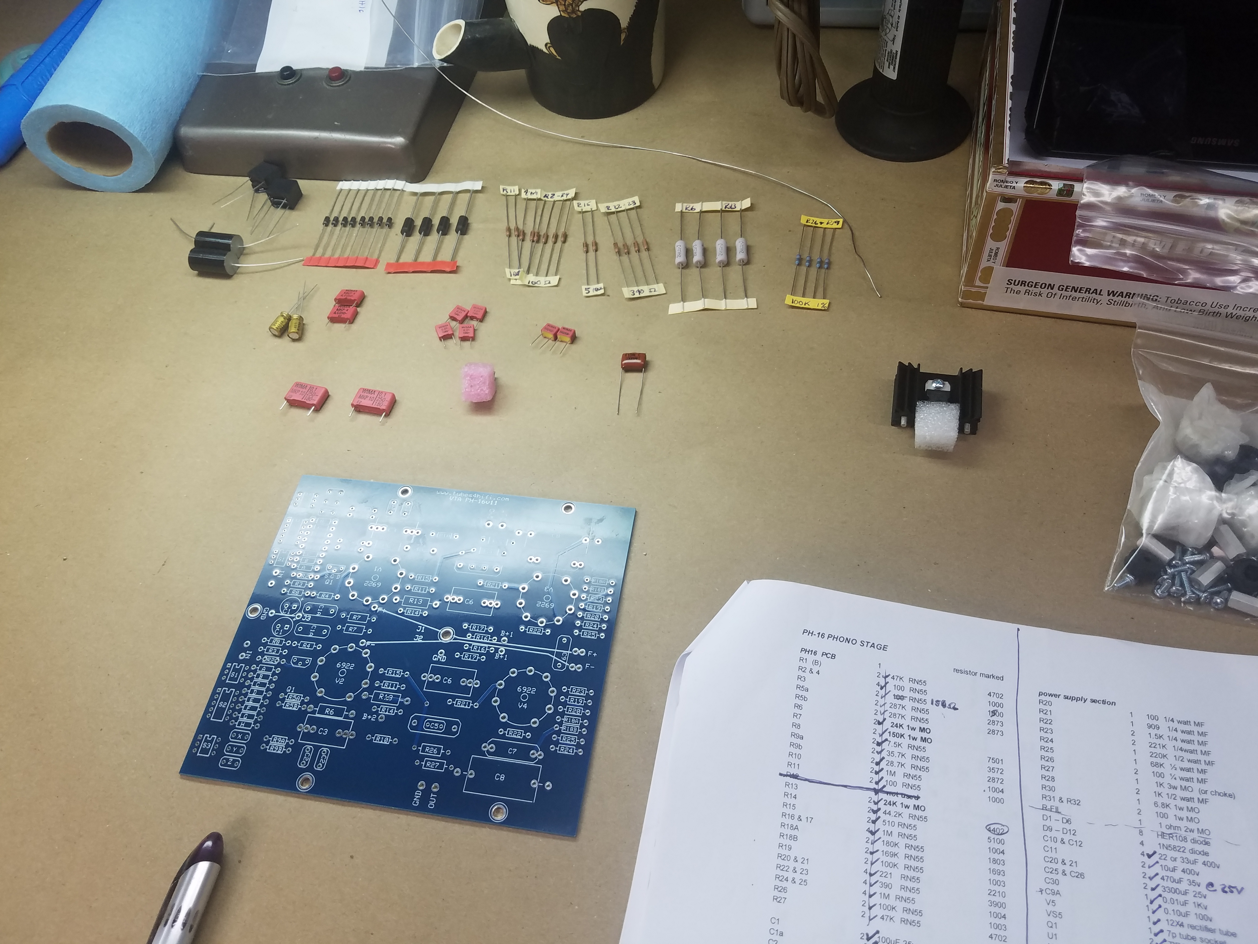
If the interest is here, I'll try to document as well as I can my build progress in this thread. Hopefully it can serve as a guide for someone who is doing their own build and give others an opportunity to learn from my mistakes and to tap the community for any help that I might need. If that goes well, I'll chronicle my SP14 build in the same fashion.
I am hosting my pics on my own server, and may take a few tries to get them to show properly. Be patient with me over the next 24 hours as I get that worked out.
This pic is the first one after I unpacked and started to lay out all of the parts before taking inventory. (If we can see it then I'll start the discussion.)
Took me a little bit, but I am closer now to having the image correct. Is it a good size or too big?
I've been a quiet member of this community for quite a while and am glad that everyone is still passionate about playing with lethal voltage for fun!
Best and more to come,
Ed in Central Texas
I would also be a fool to not mention how awesome it was to work with Kevin from Dynakit Parts too...couldn't have built my MKIIIs without him.
Last edited by edgobb on Tue Oct 01, 2019 9:04 pm; edited 4 times in total